Nios IDE CPU Detection
Hi, I am trying to create bsp and software for Nios V , using Eclipse IDE. When specifying a new projcet and its .sopc file i see message CPU not detected. And i also see message the NIOS_EDS environment variable not set. See screen shot attached . I verified via command prompt the environment variable is set and can be verified. Also i noticed there are no examples installed at this path : C:\intelFPGA_lite\24.1std\nios2eds Looking forward to resolve these issues, Thanks, Regards,45Views0likes4Commentsnot able to use multiple niosV cores at the same time
when I run ultiple niosV cores at the same time im not able to acess each of them even though i am able to detect them , i am faced with even though detecting gives me and i am unable to use the cores likewise this is my file on platform designer167Views1like7CommentsNios V/m JTAG run‑control HALT fails — Debug Module healthy, hart never halts
## Summary On a Nios V/m soft processor, JTAG **halt** never succeeds: the Debug Module enumerates and answers DMI cleanly, the hart runs and is resettable via `ndmreset`, but a `haltreq` is ignored — `dmstatus` stays `0x00400cc3` (`allrunning=1`, `allhalted=0`) indefinitely. `niosv-download`, Intel's OpenOCD build, and the Ashling RiscFree GDB server **all** fail identically with *"Could not halt the target: timeout occurred"* / *"Unable to halt … Hart 0 failed to halt during examine"*. ## Environment - Quartus Prime **Pro 26.1** (Build 110). - Nios V/m IP `intel_niosv_m` (unit `intel_niosv_m_unit_2600`, debug submodule `intel_niosv_dbg_mod_210`). - Device: Arria 10 **`10AX022C4U19E3SG`**. - Programmer: **USB‑BlasterII** (cable index 2). Single device on the chain (`JTAG ID 0x02E220DD`). - CPU clock: IOPLL `outclk0` = **100 MHz**, PLL locked (verified). Design Fmax = 131.6 MHz (timing met). ## Symptom (verbatim) ``` Internal error. Could not halt the target: timeout occurred (Ashling ash-riscv-gdb-server) Error: Unable to halt. dmcontrol=0x10000001, dmstatus=0x00400cc3 Error: Fatal: Hart 0 failed to halt during examine (Intel OpenOCD) ``` ## Direct DMI evidence (via OpenOCD `aji_client`, low‑level `dmi_read`/`dmi_write`) - SLD node enumerates: `jtagconfig -n` → `Node 08986E00 Nios V #0`. - `dmstatus` (running) = `0x00400cc3` → version=3, authenticated, **anyrunning/allrunning=1, allhalted=0**. - `abstractcs` = `0x08000002` → **progbufsize=8, datacount=2, cmderr=0** (DM healthy). - `sbcs` = `0x00000000` → **no System Bus Access** in this DM. - Direct `dmcontrol = 0x80000001` (haltreq + dmactive) → `dmstatus` stays `0x00400cc3` (**allhalted never asserts**). - `ndmreset` **works**: asserting it sets `dmstatus` havereset bits (→ `0x004c0cc3`); the hart resets and resumes. - `hasresethaltreq = 0` (halt‑on‑reset not implemented — separate facility, not the cause). ## Exhaustively ruled out | Hypothesis | Result | |---|---| | CPU clock wrong | Fixed/verified 100 MHz, PLL locked | | Timing closure | Met (Fmax 131.6 MHz) | | JTAG TCK rate | Tried 24 MHz → 6 MHz (`jtagconfig --setparam … JtagClock`) — no change | | Debugger choice | `niosv-download` = Intel OpenOCD = Ashling RiscFree — **identical** failure | | Command timeout | 120 s configured; manual `haltreq` inert | | `Enable Reset from Debug Module` | Enabled + `dbg_reset_out→ndm_reset_in` looped → `ndmreset` works, **halt still fails** | | `instruction_manager → dm_agent` mapping | Added; no effect (and PD won't place it in the instruction map) | | Stale/composed IP generation | **Removed and re‑added a FRESH `intel_niosv_m` (enableDebug=1, enableDebugReset=1), full reconnect + regenerate + recompile → identical failure** | ## Conclusion / request A correctly‑configured, freshly‑generated Nios V/m core does **not** enter Debug Mode on `haltreq` on this device/toolchain, although the Debug Module is fully responsive over DMI and `ndmreset` works. Per the RISC‑V External Debug spec, an *available* running hart must halt within <1 s of `haltreq`; this one never does. The fault appears to be in the **hart‑side debug (Sdext) halt path** of the Nios V/m IP for this version/device, or a board‑level JTAG halt‑path issue. **Questions for Intel/Altera:** - **Q1.** Is there a known erratum for Nios V/m where the DM enumerates/answers DMI but the hart ignores `haltreq` (`allhalted` never asserts)? Fixed in a specific Quartus Pro / Nios V IP version? - **Q2.** Beyond `Enable Debug`, is any parameter/connection required for the hart to honor `haltreq`? - **Q3.** Any documented Arria 10 `10AX022C4U19E3SG` JTAG/SLD interaction with Nios V run‑control halt? Related (please confirm whether either covers this *post‑enumeration* halt timeout): Intel KB **000096654**; community thread **1404335**. (KB **000096246** is a different *detection*-only defect — not this.)78Views0likes3CommentsSysID Timestamp
Hi, I would like to get the timestamp using the System ID Peripheral IP (v 19.1.8) which is connected to NIOS-V IP (26.0.0). I am using Quartus Prime Pro version 25.1.1. Using the NIOS program I am able to correctly access and print the System ID parameter that has been configured, but the returned timestamp seems to be wrong (printing: Tue Feb 4 18:03:27 2003, instead of today's date). Would you please advise if I am making any mistake in accessing the SysID timestamp, and if there is any other configuration that needs to be done on the IP? Following is my code running on the Nios-V processor and the corresponding printout.64Views0likes2CommentsImplementing many Nios® V cores on Agilex™ 7
Table of Contents Introduction Environment Configuration (HW) Configuration (SW) Mass Implementation Multicore Debugging Conclusion Note: This article is an English translation of this Japanese article by Macnica. Please refer to the original article for updates. Introduction The attention to RISC-V has been increasing year by year, and it seems that many manufacturers are developing based on RISC-V. The Nios® V I use this time is also one of the RISC-V based processors, and it is a softcore processor developed by Intel. This article is an experimental article about implementing Nios® V to the limit on Agilex™ 7, thinking about doing something interesting with RISC-V. Environment This time, since we are using Intel FPGA and Nios® V, we will use the following: Intel® Quartus® Prime Pro Edition Software Version 22.2 for Windows Ashling* RiscFree* IDE for Intel® FPGAs We will use the following for Agilex™ 7: Agilex™ 7 FPGA F-Series Development Kit (P-Tile and E-Tile) Configuration (HW) This time, to implement many Nios® V, we have created a submodule with Nios® V, and are instancing that module in the top level. The configuration of the submodule includes: Nios® V/m processor On Chip RAM JTAG-UART These three are the minimum requirements for operation confirmation. The top level includes: CLK Reset Submodule (Nios® V) ISSP Reset You may not be familiar with ISSP, but understand that we are using HW logic with ISSP to toggle the Reset because the development kit used this time does not have a reset button for FPGA. The block diagram of this configuration is as follows. (Orange is Bridge, and purple is IP, color-coded.) In this configuration, the On chip RAM for Nios® V execution memory is generated with 128kByte. For details, please refer to the capture of the Platform Designer in "Mass Implementation". This time, since we will not perform a standalone operation confirmation, we have constructed it to only run the elf file in RAM with a debugger without considering detailed settings such as Reset Vector or Boot methods for each Nios® V. Configuration (SW) The software is a simple program that outputs to the JTAG console. Since we implement multiple Nios® V, it is better to write the program so that the outputs from different cores can be distinguished. Please refer to the final outputs at the end of section Multicore Debugging. Mass Implementation This configuration is created in Platform Designer. Since we only need to instance the submodules in the top level, we are lucky that the top level remains clean, although it took time to generate. First, let's check with only one Nios® V. As explained earlier, it appears that only one Nios® V submodule is implemented in the Platform Designer system. Below is the top level system diagram (the red frame is the Sub module). This is the Sub Module (the red frame is Nios® V/m processor). The compilation result is below. Even though we used 128kB Onchip RAM, it is still only 1% utilized. Next, let's try with 10 units. To make it easier later, we have created a submodule that implements 10 submodules and instance it in the top level. Below is the compilation result. Roughly, the RAM block usage is 1% per Sub module. Let's go bold and implement 100 units. We barely managed to implement it! It's okay to implement 100 units!! Although we think we can implement a few more, as the RAM resources are over 90%, we will settle with 100 units for now. Multicore Debugging Finally, I would like to write about debugging when implementing multiple units. For the Nios® V development environment, we use Ashling* RiscFree* IDE for Intel® FPGAs introduced in Chapter 2. It can be downloaded together with Intel® Quartus® installer, so please install it together. Here, I will omit the steps for launching Ashling* RiscFree* IDE for Intel® FPGAs and importing the project. The build process was referenced from the article below: Development Procedure for Nios® V Projects using Ashling* RiscFree* IDE for Intel® FPGAs After you have built the projects, first create a Debug configuration for each CPU. You can select which CPU to create for from the Core selection in the Debugger tab, as shown below. After setting and creating the Debug configuration for each CPU, group them with Launch Group to execute them simultaneously. This completes the Debug configuration. Next, prepare the console output destination. This time, due to screen display limitations, we will display the output in each Nios® V command shell. Launch the Nios® V command shell for each CPU and execute the following command: #juart-terminal -c <change for each CPU> -d <device number> -i <instance number> juart-terminal -c 1 -d 0 -i 0 With this command, each Command shell will be linked to the JTAG console. (The last number in Core selection corresponds to the argument of -i.) Select the Group created earlier and press Debug. By default, it will break at the start of the main function, so you can add breakpoints, check register and variable values for each source to debug. The execution result this time is shown below. We captured the situation where the JTAG console is running simultaneously. Conclusion This time, I implemented many Nios® V just for fun, but it took a lot of time for tasks such as compilation time and Platform Designer hierarchy design. It was quite difficult for an article started with a light heart. However, since I think there are few people who actually perform this configuration, I hope you will find the multicore debugging part helpful. Notices & Disclaimers Intel technologies may require enabled hardware, software or service activation. No product or component can be absolutely secure. Your costs and results may vary. © Intel Corporation. Intel, the Intel logo, and other Intel marks are trademarks of Intel Corporation or its subsidiaries. Other names and brands may be claimed as the property of others. The products described may contain design defects or errors known as errata which may cause the product to deviate from published specifications. Current characterized errata are available on request. Intel disclaims all express and implied warranties, including without limitation, the implied warranties of merchantability, fitness for a particular purpose, and non-infringement, as well as any warranty arising from course of performance, course of dealing, or usage in trade. Nios is a trademark of Intel Corporation or its subsidiaries.2.8KViews0likes2CommentsNIOS II "Verify failed" for on-chip memory 128k
Hello! I'm using a Cyclone 10LP FPGA 10CL055YU484I7G FPGA. I have a 11k size program for NIOS II. I have a large on chip RAM (because I have a larger program which I want to use later) of 128k. Everything compiles and links OK. But when I try to download the program I get a "Verify failed between address 0x20000 and 0x2FFFF". The 128K memory is located 0x20000 to 0x3FFFF If I reduce the RAM to 32K, for example, everything works great!!. The initialize memory content option is turned on for the memory The BOOT RAM starts at 0x00000 If I download a bigger program (117k), I still get the same error. Thanks106Views0likes3CommentsNIOS V/m dbg_reset_out signal (Q25.1 Std, MAX10)
Hello, I have a problem with loading elf file. Signal dbg_reset_out (used for resetting HDL components) is inactive (low) when I'm using "niosv-download -r -g exeFile.elf" command (Q25.1 Std, v25.2.1 Ashling GDB Server, Linux OS, MAX10 device, NIOS V variant m). The same command for Q24.1 Std (previous version of Ashling GDB Server, the same OS and PC) works. For me temporary solution is using additional option -o (OpenOCD instead of Ashling ® RiscFree GDB Server). Is there any better solution?Solved386Views0likes14CommentsNIOS-V QSYS Warning Properties (associatedClock) have been set on
Hello, I have a really basic setup of a NIOS V system, but get Warnings in QSYS (using Quartus 25.1 Standard) about Properties of associatedClock: System: Warning: Warning: nios_subsystem.intel_niosv_m_0: Properties (associatedClock) have been set on interface reset - in composed mode these are ignored Warning: nios_subsystem.intel_niosv_m_0: Properties (associatedClock,associatedReset) have been set on interface instruction_manager - in composed mode these are ignored Warning: nios_subsystem.intel_niosv_m_0: Properties (associatedClock,associatedReset) have been set on interface data_manager - in composed mode these are ignored Questions: What is "composed mode" and how can I control it? There is no NIOS Parameter associated with it This appears in a basic setup simply by adding NIOS V to the system. How do I get rid of this warning? best regards FabianSolved179Views0likes4CommentsDK-DEV-AGI027-RA: JTAG chain broken after Nios V Hello, FPGA recovery fails
Hello, I am using the following board and host environment: Board: Agilex 7 FPGA I-Series Development Kit, DK-DEV-AGI027-RA Serial number: 8100604 Quartus Prime Pro: 25.3.1 Host OS: Windows 11 Pro Before this issue, the board was working normally with CXL ED and PCIe designs. Issue summary After successfully running a modified version of the "Nios V Hello" tutorial design (SOF + ELF) on this kit, Quartus Programmer can no longer detect the JTAG chain reliably. "Auto Detect" fails, and the JTAG Chain Debugger reports unknown devices and possible JTAG signal issues. Steps and observations 1. I modified the Nios V Hello tutorial design (SOF + ELF), including pin assignments and power management & SmartVID assignments, to match DK-DEV-AGI027-RA. Programming completed successfully, and I confirmed the expected "Hello" output. After that first run, I attempted to download an updated SOF, but Quartus Programmer "Auto Detect" failed. JTAG Chain Debugger screenshot: Programmer/Debugger log: !Error: JTAG chain problem detected !Error: TDI connection to the first detected device UNKNOWN_00000001 might be shorted to GND !Error: The TCK and TMS connections to the device before the first detected device UNKNOWN_00000001 might have a problem !Info: Detected 2 device(s) !Info: Device 1: UNKNOWN_00000001 !Info: Device 2: UNKNOWN_020D10DD Recovery attempts and results 2. Connected an external USB-Blaster II to J10, set SW8.3 = ON, and completed MAX10 recovery successfully. 3. Set SW8.3 = OFF to attempt FPGA recovery. Quartus Programmer Auto Detect still failed. 4. Loaded the predefined fpga_recovery.cdf and attempted to program AVSTX8.pof, but it failed with: Error(209062): Flash Loader IP not loaded on device 2 Error(209012): Operation failed 5. Set SW8.2 = ON to remove the FPGA from the JTAG chain, then successfully programmed AVSTX8.pof into QSPI. 6. Set SW8.2 = OFF again, but Auto Detect still failed. 7. Removed the external USB-Blaster II and tried the embedded JTAG interface. Auto Detect still failed. Questions. Are there additional recommended steps beyond MAX10 recovery and programming the recovery POF to QSPI (for example, specific switch combinations, a required full power-cycle sequence, or other board-level recovery steps)? If MAX10 recovery completes but JTAG remains broken on both external and embedded JTAG, does this suggest a likely hardware issue (JTAG path, FPGA, or related circuitry) that requires RMA? Is there anything in the Nios V Hello tutorial flow that could plausibly cause this condition (for example, power management settings, pin assignments, or JTAG-related settings)? If needed, I can share additional logs, exact switch settings, and any other diagnostics you recommend. Thanks.484Views0likes13CommentsAshling RISC Free IDE fails to download ELF file
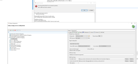
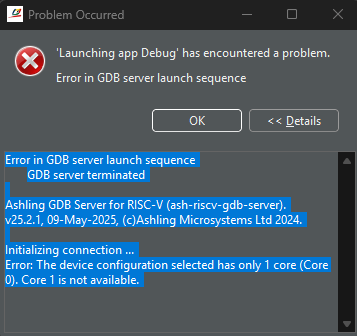
Hello ALTERA NIOSV Experts, I have been trying to execute an application using a NIOSV CPU with the Ashling RISC Free IDE. The problem is that when trying to download the elf file to a MAX10 ALTERA Development board i see an error message saying that the AShling IDE cannot determine the JTAG clock speed. I have added a Screen shot showing this event. Can anyone please suggest a solution to try ? I am currently using an ALTERA USB Blaster to connect but i have just ordered a USB Blaster II as i believe that can connect at faster clock speeds and is also more reliable. Thanks for any help,437Views0likes13Comments