fpga dev tools quartus® prime software pro
4334 Topics
Why I can't change the device family in Power and Thermal Analyzer?
Description Due to a problem in the Quartus® Prime Pro Edition Software version 26.1, you may not be able to change to a different device family in Power and Thermal Analyzer (PTA) after you create or open a design. For example, if you open a design targeting a Stratix® 10 device, you may not be able to change to an Agilex® FPGA device. In version 26.1, if you select File > New File to create a new PTA design, the new file wizard does not appear. Without the wizard, you cannot select a different device family when creating a new file. Resolution PTA locks a design to the device family selected when the file is created. To explore power consumption across different device families, create a new PTA file in the target family and import your existing design. To import an existing PTA design into a different device family: Create a new PTA file targeting the desired device family. Use the Import function to bring your existing PTA design into the new file. If you chose the wrong device family when creating a file, close the existing file and create a new one. In the File menu, select New File, and select the correct device family in the new file wizard. In version 26.1 of Power and Thermal Analyzer, the new file wizard does not appear when you select New File. To work around this issue, exit and restart PTA. After restarting, select File > New File to open the new file wizard and select the correct device family.487Views2likes0CommentsWhy does Quartus® Prime Pro give an error when trying to route HPS reset signals, such as s2f_rst or s2f_cold_rst, to the Fabric using the localized Sector Clock Network?
Description Due to device architecture requirements in Altera® SoC FPGA families with a Hard Processor System (HPS), the Quartus® Prime Pro Edition Software version 25.3.1 reports a fitter routing error when you try to route certain HPS-to-FPGA reset signals to the FPGA fabric using the localized Sector Clock Network instead of the Global Clock Network. In the Agilex® FPGA architecture, there is a device-wide Global Clock Network (meant for high fan-out signals) and a localized Sector Clock Network (meant for low fan-out, smaller regional scope, or localized logic structures). Certain signals, such as s2f_rst or s2f_cold_rst, are restricted to be only on the Global Clock Network. For example, if you use: set_instance_assignment -name GLOBAL_SIGNAL OFF -to ...|hps_inst|s2f_cold_rst Quartus reports an error similar to: Error (170084): Can't route signal "...|hps_inst|s2f_cold_rst" to atom ... Resolution Certain signals, such as s2f_rst or s2f_cold_rst, are restricted to be only on the Global Clock Network. To work around this routing error in the Quartus® Prime Pro Edition Software: Remove any instance assignment that sets GLOBAL_SIGNAL to OFF for HPS-to-FPGA reset outputs (for example, s2f_rst or s2f_cold_rst). Recompile the design and allow Quartus to route these reset signals on the Global Clock Network. This behavior reflects device architecture and fitter rules; it is not scheduled to be changed to allow HPS-to-FPGA reset signals on the Sector Clock Network.55Views0likes0CommentsWhy does the SystemConsole.refreshMasters DSP Builder function fail?
Description When using the SystemConsole.refreshMasters DSP Builder function in the Quartus® Prime Pro Edition version 26.1.1 and above, you may see the following error: Unable to resolve the name 'com.altera.systemconsole.matlabapi.SystemConsoleLink' This error occurs because the Java version used by MATLAB is incompatible with com.altera.systemconsole.matlabapi.SystemConsoleLink. For DSP Builder version 26.1.1 and later, MATLAB must use Java version 11 or later for SystemConsole.refreshMasters to run successfully. Resolution You can change MATLAB's Java version using either the jenv MATLAB function or the matlab_jenv executable. For information on how to use jenv and matlab_jenv, refer to the MATLAB documentation.39Views0likes0CommentsWhy does Quartus® Prime Pro report Error (26193) and a Fatal Error in ddm_module_iters.cpp during Synthesis for F-Tile designs with secure MIFs?
Description Due to a problem in the Quartus® Prime Pro Edition Software version 26.1.1, Synthesis may fail on Agilex® 7 FPGA F-Tile designs that use secure Memory Initialization Files (MIFs) when hierarchy paths contain period (.) characters introduced by RTL generate blocks. The Quartus® Prime Pro Edition Software incorrectly treats periods inside generate-block instance names as hierarchy separators. As a result, the tool cannot resolve the secure MIF hierarchy path, reports Error (26193), and then terminates with a fatal assertion. Resolution To fix this problem in the Quartus® Prime Pro Edition Software version 26.1.1, install patch 1.03 below for the correct OS. This problem is scheduled to be fixed in a future release of the Quartus® Prime Pro Edition Software.145Views0likes0CommentsError: The “…/script/../niosv_software/dp_demo_bsp/settings.bsp file does not exist
Description Due to a problem in the Quartus ® Prime Pro Edition Software version 26.1, the generated DisplayPort example design for Stratix® 10 FPGA does not contain the correct BSP file. The command “quartus_py .\build_niosv_sw.py -d” mentioned in DisplayPort Stratix® 10 FPGA IP Design Example User Guide does not regenerate correct BSP file either, which causes the error “Error: The “…/script/../niosv_software/dp_demo_bsp/settings.bsp" file does not exist”. Resolution To fix this problem, execute “quartus_py ./build_niosv_sw.py -d -b” instead to regenerate .elf file. The “-b” option is only necessary for the first run.105Views0likes0CommentsWhy are there no example design options available in the “Select Design” drop-down list in the DisplayPort IP Parameter Editor GUI?
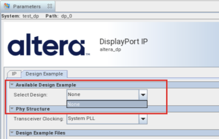
Description Due to a problem in the Quartus ® Prime Pro Edition Software version 26.1, the drop-down list for “Select Design” in the Display Port IP Parameter Editor GUI only has “None” option, as shown in the screenshot below. Resolution This problem has been fixed beginning with version 26.1.1 of the Quartus® Prime Pro Edition Software.166Views0likes0CommentsError: (vlog-7) Failed to open design unit file
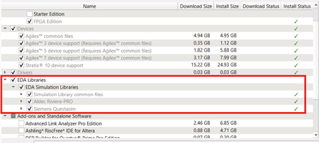
Description Due to simulation models not being installed along with the Quartus ® Prime Pro Edition Software, an error such as: Error: (vlog-7) Failed to open design unit file "C:/altera_pro/26.1.1/quartus/eda/sim_lib/220model.v" in read mode may occur during simulation. The root cause of missing files is that “EDA libraries” are not installed properly during installation of the Quartus ® Prime Pro Edition Software. Resolution To fix this problem, make sure “EDA Libraries” has been checked and installed properly during installation of the Quartus ® Prime Pro Edition Software, as shown in the screenshot below.94Views0likes0CommentsWhy does the Agilex® 5 DisplayPort SST TX-Only example design fail to generate when AXIS-VVP Full is enabled?
Description Due to a problem in the Quartus® Prime Pro Edition Software version 25.3 and earlier, you might see the following example design generation errors when generating the Agilex® 5 DisplayPort SST TX-Only example design with AXIS-VVP Full enabled. error: 'VVP_TPG_BASE' undeclared (first use in this function) Error: Failed to generate example design example_design to: <example_design_path> Resolution This problem is scheduled to be fixed in a future release of the Quartus Prime Pro Edition Software.44Views0likes0CommentsWhy am I unable to run BKP operations with Quartus® Prime Pro Edition 26.1.1 on Windows*?
Description Due to a problem in the Quartus® Prime Pro Edition Software version 26.1.1, Black Key Provisioning (BKP) operations might fail on Windows* with the following error: Error: BKP PLUGIN: [3000] Http error: Could not use specified SSL cipher because Quartus has enabled the Windows SSP interface Schannel (Secure Channel) to work with the OpenSSL library. When using libcurl with the Schannel (Windows) backend, the option CURLOPT_SSL_CIPHER_LIST does not accept individual, specific cipher suites (for example TLS_ECDHE_RSA_WITH_AES_256_GCM_SHA384). Resolution To work around this problem in the Quartus® Prime Pro Edition Software version 26.1.1, build a patched bkpprog.dll and select it through the project configuration, as follows: 1. Clone the source repository: GitHub - altera-fpga/device-security-software-services: Device Security Software and Services source code for FPGA Device Onboarding, Attestation, Secure Session, Black Key Provisioning. 2. Prepare the Windows build environment. Follow the Windows Build instructions in the repository README. Install the listed prerequisites and prepare the repository dependencies exactly as documented there. 3. Modify network_wrapper.cpp. Open the following file in the cloned repository: bkpprogrammer/src/core/cpp/network/network_wrapper.cpp In CurlWrapper::CurlWrapper, locate the TLS version and cipher-list configuration: setCurlOptionWithErrorHandling( curlHandle, CURLOPT_SSLVERSION, CURL_SSLVERSION_TLSv1_2); setCurlOptionWithErrorHandling( curlHandle, CURLOPT_SSL_CIPHER_LIST, acceptedCiphers.c_str()); Replace it with: setCurlOptionWithErrorHandling( curlHandle, CURLOPT_SSLVERSION, CURL_SSLVERSION_TLSv1_2); 4. Build the patched plug-in. Return to the repository root and build by following the repository Windows Build instructions. Confirm that bkpprog.dll is regenerated after network_wrapper.cpp was modified. 5. Place the custom plug-in. Create the following directory under the BKPS project and copy the rebuilt bkpprog.dll into it. Do not replace the DLL inside the Quartus installation. <project>\cm_provisioning\bkp_plugin\bkpprog.dll 6. Create quartus.ini. Create a quartus.ini file directly under the project cm_provisioning directory with the following line: PGM_ALLOW_CUSTOM_BKP_PLUGIN=7S6Nh0s3@on 7. Update bkp_options.txt. Use the normal project-specific BKP values and add bkp_plugin with the path to the rebuilt DLL: bkp_cfg_id = <ID> bkp_ip = <IP> bkp_port = <PORT> bkp_tls_ca_cert = "<Path_To_bkps_ssl_cert.crt>" bkp_tls_prog_cert = "<Path_To_pro_cert>" bkp_device_opn = <OPN> bkp_plugin = "<Path_To_bkpprog.dll>" 8. Run Quartus Programmer where quartus.ini is located. Set the current working directory to the cm_provisioning directory that contains quartus.ini and bkp_options.txt. Quartus reads quartus.ini from its current working directory, so run the commands from here: quartus_pgm.exe -c 1 -m jtag --bkp_options=bkp_options.txt --bkp_prefetch Use the same working directory for Set Authority and Provision operations, so Quartus continues to load the custom plug-in setting from quartus.ini. This problem is scheduled to be resolved in a future release of the Quartus® Prime Pro Edition Software.54Views0likes0CommentsWhy does the Quartus® Prime Pro Edition Software report a pin placement error when Customize Pin Selections is disabled in the LVDS SERDES IP?
Description When using the LVDS SERDES IP with Agilex® 5 FPGAs or Agilex® FPGA 7 M-Series FPGAs, the physical byte and pin assignment must match the pin index specified under the Pin Settings tab in the IP Catalog GUI. If a physical byte or pin is selected without matching the corresponding pin index, the Quartus® Prime Pro Edition Software may report a pin-placement or compilation error. Even when Customize Pin Selections is not selected, each pin must be assigned according to the default byte and pin values specified for its corresponding pin index in the Pin Settings tab. Not selecting this option does not allow arbitrary byte or pin assignments. To use a different byte and pin assignment, select Customize Pin Selections and manually assign the byte and pin locations according to the design requirements and the supported device pin mapping. Resolution To avoid this problem, assign the LVDS SERDES IP pins according to the specified pin index in the Pin Settings tab; to use a different byte and pin assignment, select Customize Pin Selections and manually assign the byte and pin locations according to the design requirements.75Views0likes0Comments