cyclone® v fpgas and socs
1057 Topics
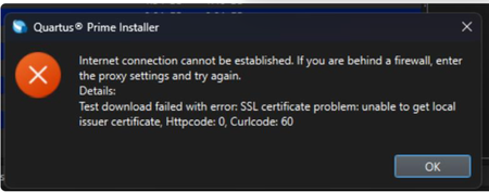
Why does my Quartus® Prime Installation fail with certificate error: SSL certificate problem: unable to get local issuer certificate (curlcode 60)?
Description Due to a problem in the Quartus® Prime Installer Software, you might see the error message shown below when you click Download & Install. This happens because the certificate bundled with the Quartus® Prime Installer Software is no longer accepted by the Altera® Content Delivery Network (CDN). As a result, secure downloads initiated during the installation process cannot be verified using the outdated certificate. The issue impacts the Installer for the following versions of Quartus software: Operating System Quartus Prime Pro Installer Version(s) Quartus Std/Lite Installer Version(s) Microsoft Windows* 23.3 to 25.3.1 23.1std to 25.1std Linux* 23.3 to 23.4 23.1std The KDB workaround provided below applies to the following versions of Quartus software: Quartus Prime Pro Installer Version(s) Quartus Std/Lite Installer Version(s) KDB workaround applies to 24.3 to 25.3.1 24.1std to 25.1std Note that for all other affected versions not covered by the KDB, you cannot use the installer workaround and must download Quartus software package files individually without using the installer. Separate packages can be found in the Individual Files tab of the Quartus Software Download pages. Resolution To work around this problem, follow these steps: 1. Download and unzip the cacert.zip, which contains the cacert.pem certificate file. 2. Specify the new certificate using one of the following methods: i) Command Line Interface (CLI): Open a command prompt or terminal and run the installer with the--cacert option, pointing to the new certificate file. Windows*: qinst_<version>.exe -sp"--cacert <full path to cacert.pem>" Linux*: qinst_<version>.run -- --cacert <full path to cacert.pem> ii) Graphical User Interface (GUI): - Open the Quartus® Prime Installer, navigate to Settings, locate the CA Certificate Path, and specify the full path to the cacert.pem certificate file. - Then, click Apply > OK. This problem is scheduled to be resolved in a future release of the Quartus® Prime Installer Software.11KViews1like0CommentsWhy does the text overlap in the ALTPLL IP Parameter Editor?
Description Due to a problem in the Quartus® Prime Standard Edition Software version 25.1, you might see that the text overlaps in the ALTPLL IP Parameter Editor on the Windows* Operating System. This prevents the ALTPLL IP from being instantiated. This problem does not occur in the Quartus® Prime Standard Edition Software version 24.1 and earlier. Resolution To work around this problem in the Quartus® Prime Standard Edition Software version 25.1, download and install the patch below: This problem is scheduled to be resolved in a future release of the Quartus® Prime Standard Edition Software.1.4KViews1like0Comments
Error: TBBmalloc: skip allocation functions replacement in ucrtbase.dll: unknown prologue for function _msize
Description Due to a problem in the Quartus® Prime Standard Edition Software version 25.1 or earlier, you might see this error message when generating PLL IP on Windows* 11 Operating System. The IP generation might complete successfully even though this error message is reported. Resolution To work around this problem, follow these steps: Go to This PC, right-click, and select Properties. Click Advanced System Setting. In the Advanced tab, select Environment Variable. Under System variables, create a new variable with the name TBB_MALLOC_DISABLE_REPLACEMENT and value as 1. Click OK and restart the Quartus® Prime Software. The workaround above does not work for the Quartus® Prime Standard Edition Software version 22.1std.2 or earlier. A patch is available to fix this problem for the Quartus® Prime Standard Edition Software version 22.1std.2. The environment variable is still required to prevent the TBBmalloc message from appearing. Download and install patch 2.02 below: Patch 2.02 for Windows (.exe) Readme for patch 2.02 (.txt) This problem is not scheduled to be fixed in the Quartus® Prime Standard Edition Software.1.1KViews1like0CommentsCan I use the INPUT_TERMINATION .qsf assignment to assign an on-chip termination (OCT) to Transceiver REFCLK or Transceiver IO pins, in Stratix V, Arria V and Cyclone V devices?
Description No you cannot use the INPUT_TERMINATION assignment to assign an on-chip termination (OCT) to transceiver pins on Stratix® V, Arria® V and Cyclone® V devices. Instead, you must use one of the following qsf assignments : XCVR_GT_IO_PIN_TERMINATION (Stratix V GT transceiver IO pins ony) XCVR_IO_PIN_TERMINATION (transceiver IO pins) XCVR_REFCLK_PIN_TERMINATION (REFCLK pins) Refer to the Altera Transceiver PHY IP Core User Guide (PDF) for more information on how to use these assignments. Note that if you use an INPUT_TERMINATION assignment on the transceiver pins, it will be ignored by the Quartus® II software and the default termination option will be assigned to these pins. Related Articles Error (169033): I/O pin with Termination logic option setting Differential cannot be placed inside I/O Bank because the I/O bank does not support the requested Termination setting.697Views0likes0CommentsHow do I interpret the Recommended Operating Conditions and Allowable Ripple recommendations of Altera devices?
Description The Recommended Operating Conditions for Devices and Allowable Ripple recommendations are separate parameters and cannot be combined. The Recommended Operating Conditions for Devices published in the device datasheets refers to the nominal DC requirement of the supply rails. The Allowable Ripple recommendations published in the Power Distribution Network (PDN) Tool refer to AC transient voltage fluctuations and are intended for PDN decoupling design. For device specific power supply recommended operating conditions, please refer to the relevant device datasheet. For device specific power supply voltage ripple recommendations, please refer to the "Introduction" tab of the device specific PDN Tool. Power Distribution Network Design Tool Related Articles Why are the device voltage supply minimum and maximum values different in the Power Delivery Network (PDN) Tool when compared to the Altera device Datasheet recommended operating conditions? How do I use the Altera PDN Tool to evaluate decoupling requirements for a MAX 10 device?600Views0likes0CommentsError : FLEXlm version of vendor daemon is too old
Description In the Questa* FPGA Edition simulator and Questa* FPGA Starter Edition simulator version 2024.1, you might see this error or the following error if you are using the MGCLD daemon v11.16.4 “Unable to checkout a license. Make sure your license file environment variable (SALT_LICENSE_SERVER, MGLS_LICENSE_FILE, LM_LICENSE_FILE) is set correctly” Resolution To avoid this error, upgrade to the Siemens* Flexlm (SALTD) daemon v11.19.5 Download the daemon from the download page There is a change to the Siemens* License in v11.19.5.0. If you’re running a floating license server for Siemens* licenses, manually change the VENDOR daemon line in the license file from mgcld to saltd, for example: VENDOR saltd <path to saltd> Note: Do not change any of the INCREMENT lines. Leave the INCREMENT lines with the original vendor daemon name (mgcld).599Views0likes0CommentsDoes the Advanced clock phase control adjustment in the HPS DDR3 work?
Description You may notice the Advanced clock phase control setting in the HPS GUI PHY Settings tab. Changing the phase value has no effect on the phase of the PLL output clocks. Resolution The Advanced clock phase control adjustment will be removed in a future version of the Quartus® II software. This problem was fixed in Quartus® II software version 13.1598Views0likes0CommentsCyclone V Device Family Pin Connection Guidelines: Known Issues
Description Issue 99877: Version 1.5 The connection guideline for HPS_CLK2 pins states "This is an optional HPS clock input pin. When you do not use this pin, Altera recommends tying it to GND or leaving it unconnected. If this pin is unconnected, use the Quartus II software programmable options to internally bias this pin.This pin can be reserved as an input tri-state with the weak pull-up resistor enabled, or as an output driving GND." The HPS_CLK2 is a dedicated input. When HPS_CLK2 is not used, it must be connecetd to GND. Issue 67591: Version 1.3 The connection guideline for VREF pins says if voltage reference I/O standards are not used in the bank, the VREF pins are available as user I/O pins. The VREF pin of Cyclone V device is a dedicated power pin, it is not allowed to be used as user I/O when voltage reference I/O standards are not used in the bank. This is fixed in coming release to reflect the correct VREF pin description. Resolution Resolved Issues: Issue 44314: Version 1.0 The connection guideline for unused GXB_RX pins says to connect to GND through a 10-kΩ resistor. The 10-kΩ resistor is un-necessary, unused GXB_RX pins can be tied directly to GND. This is fixed in version 1.2.500Views0likes0CommentsWhen does the Quartus® Prime Design Software, IP cores, and Questa*-Altera® FPGA Edition Software check out a license?
Description Below is a description of how the Quartus® Prime Design Software, IP cores, and Questa*-Altera® FPGA Edition Software utilize licenses: Resolution Quartus® Prime Design Software: All Quartus® Prime Design Software processes check for a valid license, including the Quartus® GUI, Analysis & Synthesis, Assembler, and TimeQuest Timing Analyzer. These processes start only if a valid license is available. They do not hold or occupy the license; they only validate that one is available. However, the Fitter checks out a license when it starts and holds it for the duration of the Fitter process. IP cores: A license for an IP core is checked out when the Quartus® Prime Design Software opens the first encrypted file of the IP core for synthesis. This license is held for the duration of synthesis. The Assembler checks out the license for every IP core to create the programming file and holds it for the duration of the Assembler process. Questa*-Intel® FPGA Edition software: Once Questa*-Intel® FPGA Edition Software loads a design unit during elaboration, a Questa-Intel® FPGA Edition license is checked out. It remains checked out until the simulation ends (quit -sim), or the simulator is closed. Once a waveform is loaded into the simulator, a Questa*-Intel® FPGA Edition Software license is also checked out for viewing Wave Log Format File (.wlf), and it remains checked out until the waveform window is closed. Related Articles What happens to a license if the Quartus II software terminates unexpectedly? Can I perform multiple compilations using the Quartus II software at the same time on one computer with a one seat floating license or one fixed (node locked) license file?500Views0likes0CommentsWhy does Linux report "DMA engine initialization failed" error when EMAC uses GMII interface?
Description When supporting GMII interface for HPS EMAC, there are three clocks exported to FPGA: emac_tx_clk_i(input), emac_rx_clk_i(input), emac_gtx_clk(output) The Linux would report below error if the emac_tx_clk_i clock is not connected correctly: ...... [ 4.291414] socfpga-dwmac ff802000.ethernet: Failed to reset the dma [ 4.297785] socfpga-dwmac ff802000.ethernet eth1: stmmac_hw_setup: DMA engine initialization failed [ 4.306806] socfpga-dwmac ff802000.ethernet eth1: stmmac_open: Hw setup failed ...... Resolution Besides connecting the emac_rx_clk_i(125MHz) for GMII, the emac_tx_clk_i also needs to be connected correctly (2.5MHz or 25MHz), although it is not used in GMII mode. The emac_tx_clk_i requirement information has been added in the HPS document beginning with version 21.2.499Views0likes0Comments