board debug
623 Topics
Cyclone V GT Dev Kit - new units fail to boot from FPP
We have been using this development kit internally for many years, and on our last order 2 out of 3 units fail to boot using the Fast Passive Parallel (FPP) configuration scheme through the MAX V. We normally use our own custom MAX V bitstream, but the issue is present even with the factory MAX V image and the factory FPGA image/flash content. The MAX V appears to try loading the image (LED D6 flashing or statically lit, depending on the MAX V firmware version) for about 6 seconds before giving up and signaling an error (LED D5). On reception, one of the two faulty boards seemed to work, it was just taking a bit longer to boot than usual (presumably it took a few retries). It then got progressively worse: the boot started failing intermittently, and now it is almost impossible to get it to boot through FPP. The boards can still boot through Active Serial (AS), and the FPGA can properly read and write the main flash, so the issue seems to affect only the MAX V flash access / FPGA configuration. Following this thread, which reports the same issue: Cyclone VGT Dev Kit boards - some new boards failing to boot from NOR Flash | Altera Community - 353984 we tried reducing the MAX V utilization to improve timing. With this change one of the boards managed to boot a few times, but very rarely and not reliably. The affected boards are all rev. B and have serials: - 5CPCIE00100214 - 5CPCIE00100263 While debugging, I also noticed that the timing constraints do not follow the Parallel Flash Loader IP User Guide. For example, fpga_dclk should be a generated clock and used as the reference for the other constraints, and the set_output_delay on fpga_data does not respect the tDSU from the Cyclone V datasheet. That said, correcting these constraints did not improve the boot behavior. We are now stuck with two boards that can only boot from AS, which is a concern for future orders. Between this and the flash revision change to rev. B (where the PCB is actually labelled rev. A and the example designs are mixed and not clearly labelled), these boards are becoming difficult to work with. Since there is at least one other thread reporting the same behavior it looks less like an isolated fault and more like a recurring issue on recent production. Could someone from Altera confirm whether this is being tracked, and what the recommended action is for affected boards?Solved315Views1like13CommentsCannot program cyclone IV with USB blaster
Hello, I have an Altera Cyclone IV EP4CE6E22C8N board which supports programming via JTAG USB, and so I have a USB blaster revision C and connected it to the JTAG port and installed the drivers for it through the Quartus Prime installer, but unfortunately every time I try to use the programmer with it plugged in, it hangs for a while then prints an error saying "Attempted to access JTAG server -- internal error code 82 occurred", running jtagconfig also says: "Error when scanning hardware - Server error", device manager also shows only USB blaster when as far as I know it should also be showing additional entries such as JTAG interface? I tried different drivers but to the same effect, reinstalling quartus prime and all the drivers, no luck. I also tried running a windows 7 VM and installing quartus prime and the programmer drivers on there in case it was a compatibility issue, but the same happens, server says "server error" and the programmer hangs. I looked in event viewer and the driver appears to be outputting errors: I have also tried to install the drivers manually through the quartus prime 23 install directory. I'm really not sure what to do anymore, hoping someone with more experience can help. Thank you! I am running Windows 11, X86 of course.Solved3.1KViews0likes8Comments
Agilex 7 R-Tile PIPE Direct endpoint receives Set_Slot_Power_Limit, but no Config TLPs
Hello, I am developing a custom PCIe endpoint using the Agilex 7 R-Tile PIPE Direct interface. The PHY is provided by the R-Tile IP, while the LTSSM, Data Link Layer, and TLP/DLLP handling are implemented in soft RTL. Environment FPGA: Agilex 7 AGIB027R29A Quartus Prime Pro 24.3.0 Build 212 R-Tile PIPE Direct mode PCIe Gen3 x8 Custom soft LTSSM and Data Link Layer Linux host with a commercial PC/root complex The FPGA is configured before a host cold boot The endpoint is not currently visible in lspci In a successful Signal Tap capture: The LTSSM reaches Gen3 L0. The Data Link Layer reaches DL_ACTIVE. InitFC1 and InitFC2 for Posted, Non-Posted, and Completion traffic are exchanged. We observe valid incoming TLP traffic with a correct LCRC. The host sends a Message TLP that appears to decode as Set_Slot_Power_Limit. No subsequent Configuration Type 0 Read TLP or other expected enumeration TLP is observed. The link later returns from L0 to Recovery.RcvrLock. Our understanding is that Set_Slot_Power_Limit is a posted Message TLP and should not require a Completion TLP from the endpoint. The endpoint should only acknowledge successful reception at the Data Link Layer. Please correct us if this interpretation is wrong. Questions Is receiving Set_Slot_Power_Limit before the first Configuration Read a normal root-port enumeration sequence? Does the endpoint need to respond to this Message TLP in any way other than sending a Data Link Layer ACK? If the ACK DLLP has an incorrect sequence number, CRC, or timing, could the root port stop sending further TLPs and eventually force the link into Recovery? Are there any R-Tile PIPE Direct-specific status or control signals that must be handled before the host starts Configuration transactions? Are there recommended R-Tile debug signals for determining why the root port stops after this message? Could an incorrect Flow Control advertisement—especially Completion Header/Data credits—cause this behavior even if InitFC2 completes? Are there known PERST#, cold-boot, or FPGA-configuration timing requirements for enumeration when using PIPE Direct mode? We are currently capturing the following signals: LTSSM state Data Link Layer state InitFC1/InitFC2 and UpdateFC status Received TLP Fmt/Type and complete header Received TLP sequence number LCRC result ACK/NAK request and transmitted ACK/NAK sequence number Replay timer/replay status RX block lock, CDR lock, and lane numbers Raw 1024-bit PIPE RX block data Any guidance on the expected transaction sequence after Set_Slot_Power_Limit, or additional signals that should be captured, would be greatly appreciated. Thank you.79Views0likes1Comment
R-tile CXL base hard IP example for the Agilex 7 M-series Dev Kit (DK_DEV_AGM039EA) does not work
We recently generated an R-tile CXL base hard IP example for the Agilex 7 M-series Dev Kit (DK DEV AGM039EA) with both Quartus Prime Pro 25.3.1 and 26.1. However, the CXL link is always down and stuck at Gen1 2.5Gbps. Do you have any suggestions, or is there a working CXL design example for this kit? We verified that the link functions perfectly with a PCIe Gen5/Gen4 example.We recently generated an R-tile CXL base hard IP example for the Agilex 7 M-series Dev Kit (DK DEV AGM039EA) with both Quartus Prime Pro 25.3.1 and 26.1. However, the CXL link is always down and stuck at Gen1 2.5Gbps. Do you have any suggestions, or is there a working CXL design example for this kit? We verified that the link functions perfectly with a PCIe Gen5/Gen4 example.90Views0likes2Comments
Cyclone VGT Dev Kit boards - some new boards failing to boot from NOR Flash
We've been using these boards for years, having certified them for use in one of our products. In the last few months we have now received 5 of these boards and they fail to configure from NOR flash. These are all the new Rev B CVGT Dev Kit edition. Not all of the new RevB fail, but the fail rate is high, getting close to 50%. Yes, we know they changed to a Micron NOR flash for Rev B and rerouted some data lines, we are using the new RevB MAX5 files and have updated the Cyclone V NOR flash pins to match as well. I made some diagnostic changes to the MAX5 boot source (I set the PGM leds to count retries) and discovered that on the bad boards, the boot process goes through multiple configuration retries and eventually the watchdog timer fires, turns on the ERR (D5) red LED and stops. With the factory image they come with, there are also dozens of retries, then sometimes the boards fail, sometimes they boot up. With the slow speed that the NOR flash configuration runs at, there is no reason that it should ever fail and retry, and indeed on good boards they configure the first time every time with no retries. The first four we were able to send back to Altera (Via digikey where we bought them). We just got another bad one yesterday, this one from Mouser. Has anyone else seen this issue, and/or heard from Altera about this? Board link: https://docs.altera.com/r/docs/792833/current/cyclone-v-gt-fpga-development-kit-user-guide/kit-features556Views1like25CommentsARM DS5 debugger Access/Detection of CM55 on Agilex5 fpga device
Hi Team, We recently purchased license for the ARM DS5 IDE from Altera with License file contains note as NOTICE="For use with Intel or Altera devices only". I am using Arm Development studio IDE with version 2025.1-1. ALtera Agilex 5 FPGA device configured with custom soft macro based design which is only having ARM Cortex M55 processor cores with coresight debug IP . My question is whether ARM DS IDE will detect, access and debug the Cortex M55 cores which is in the fpga through the JTAG USB Blaster ? Please provide the detailed explanation Regards Suresh139Views0likes13Comments
Brand new USB-BLASTER 3 issues
A day ago I received a brand new and very expensive USB Blaster III from DigiKey with the following Serial Number: UB3000432 I have an issue using this device. The device is visible both in Win11 Device Manager and Quartus Prime Pro 26.1. After the device is properly connected to the PCB (I’ve tested 3 different boards) and powered on, the JTAG link is not established. All connections are correct, pinouts are aligned, and I even checked the conductivity of wires from board to Blaster module. I've managed to get this log from Quartus: !Error: JTAG chain problem detected !Error: No device detected. Detected 1's at TDI pin. The thing is that this same boards (chips) are visible to older USB Blaster in the same configuration. This was a sanity check. Am I missing something that is not documented in the user manual? Best regardsSolved229Views0likes8Comments
JTAG pins order for USB Blaster III - 1.27" header
USB Blaster III header has shrined in size relatively to the previous JTAG cables. I see that in addition, pinout order has changed(according to USB Blaster III user guide). So, if I want to place on a new board that I'm developing a matching connector(pitch=1.27") for USB Blaster III (without using the adapter board from the KIT), then I have to use new pinout order: 1-VCC_TRGET, 2-TMS, 3-GND, 4-TCK, 6-TDO, 7-nTRST, 8-TDI, 9-GND, 10-nPROCRST. This order is different then was used with previous JTAG cables. I couldn't find any reference schematic(also of EVAL KITs) that supports this new JTAG order. I will appreciate if anyone from the forum can confirm my observation. If it's possible that someone can answer me with an existing working reference design with 1.27" connector, I will appreciate it more.81Views0likes1Comment
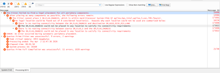
Fitter error in A5ED043AB23AI2V Example design
Hi, I have tried using the example design of the A5ED065BB32AE4SR0 development kit and modified the part number to A5ED043AB23AI2V. During compilation, I am encountering a fitter error when both PCIe and USB 3.1 are enabled together. However, I am able to compile successfully when using each interface individually. Could you please help me understand how to resolve this issue?144Views0likes6Comments