
BrianSune_Froum Contributor
ContributorCyclone V SoC 5CSXC6 Series GXB Utilization and Limitations
 Contributor
 Regular Contributor
Hi Brian,
Thanks for your update, and apologies for any confusion.
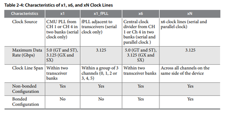
Based on the Cyclone V Device Handbook Volume 2: Transcievers -> Table 2-4: Characteristics of x1, x6, and xN Clock Lines, each fPLL can only drive a group of three channels (0–2 or 3–5). This is due to the fPLL clock line span is within a group of 3 channels (0, 1, 2 or 3, 4, 5).
Since the remaining channels are CH2, CH3, and CH5 (spanning both groups), two fPLLs would be required to cover them.
Please let me know if you have any further questions.
Thank you.
 Contributor
CheepinC_altera
I will get back to you after testing
CheepinC_altera
Quick fitting test shows:
PCIe X2 GEN 1 (max speed on this device) + Custom x2 protocol < (3.125Gbps)
Can be placed on [Ch0+Ch1(Ch4)] + [Ch3,Ch5]
Total GXB usage 4
So simply speaking
The maximum possible GXB can only be 5 and never 6?
I still don't get it: Why channel 4 cannot be used as TRX when CMU PLL is placed.
Aren't the internal function block supposed to be stand alone?
Meantime, from the above test result:
For PCIe x4 the expected Ch5 can be placed by fPLL.
So the best cases are Total of 5 TxR channels?
Additional placement view info:
You can see it is completely empty for use but why CMU use case make if unusable?
Meantime the GXB TX use case shows a very distinct placement.
It is very "Counterthinking" on this fitter idea!!!
Thanks,
Brian
Regular ContributorHi Brian,
Thanks for your update. Please allow me sometime to look into your latest response. I will get back to you by early next week. Please ping me if you do not hear back from me. Thank you.
ContributorLSS: The goal here is to find the possible usage or maximum usage on these GXB.
PCIe is a must the reduction to x2 is also good enough as x4 itself do not really gain much BW via HPS.
So if possible x4 on remain GXB is what we expected.
bottom [0|1] <- PCIe x2
bottom [2] + top[3|5] [4] ? 4 channel via fPLL x2 ??
Regular ContributorHi,
Thank you for the update. Based on my understanding, you are planning to implement the following configuration:
From a theoretical standpoint, this configuration appears feasible. I would recommend creating a small test design and running it through the Fitter to verify compliance with any internal placement rules.
Please let me know if you have any questions or if there are any concerns. Thank you.

