 Occasional Contributor
How to define timing constrains for input and output
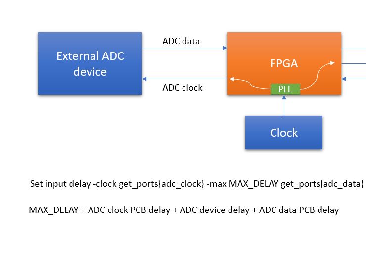
If I look the timing analysis user guide, it recommend to use virtual clock to define timing constrain for input and output. But I don't know what's the difference between using virtual clock and clock from FPGA port. Could you use below example to explain a little? Thanks a lot!
A virtual clock is used for I/O timing analysis. It's created using the create_clock constraint and describes the clock that launches data for an upstream device (an input to the FPGA) or the clock that latches the data for a downstream device (from an output of the FPGA). It's called virtual because it has no target because it never actually enters the FPGA itself. Your set_input_delay and set_output_delay constraints always reference the virtual clock (except for some unique circumstances like source synchronous clocks).
To learn more, see this online training:
https://www.intel.com/content/www/us/en/programmable/support/training/course/odsw1118.html
If you are talking about source synchronous interfaces, where the clock is generated by the upstream device or the FPGA generates the clock to be sent to a downstream device, see these trainings, depending on whether you're talking about single data rate or double data rate:
https://www.intel.com/content/www/us/en/programmable/support/training/course/ocss1000.html
https://www.intel.com/content/www/us/en/programmable/support/training/course/oddr1000.html
