
BrianSune_Froum Contributor
ContributorCyclone V SoC 5CSXC6 Series GXB Utilization and Limitations
 Contributor
 Regular Contributor
Hi Brian,
Just to update you that I am still running tests using Native PHY designs to check the placement rules. Could you please share the test design that reproduces the reconfiguration placement issue? I would like to replicate the issue on my side and continue debugging from there.
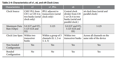
Regarding your question on “why the PCIe IP requires CH4 instead of CH1 in the first place”: If I understand you correctly, you are asking why, in PCIe x2 mode, CH4 RX is required as the CMU PLL. If so, for clarification, the CMU PLLs in CH1 and CH4 also function as the CDRs. When PCIe x2 uses CH0 and CH1, there is no additional CMU PLL available in CH1. As a result, the design must use the CMU PLL in CH4.
Please let me know if I misunderstood your question or if you need any further clarification. Thank you.
 Contributor
I can only share the IP from altera all other logic and block will be cropped if this is ok for you I will cont'd to do so.
Q: I think the major issue here is reconfiguration block 1 -> top 1->bottom only 1 on each.
so if the reconfiguration block already hold by PCIe there is not way additional transceiver can run on different speed unless it is same as PCIe spec.
So before we spend time on this maybe have a look on Q:
I am not sure you are altera FAE staff or just regulator forum contributor?
However, I think if you have idea have to do it you should able to use this to validate what we are discussing.
Fair enough for my side to provide this and I cannot see why there are no easy test on your side to validate this as well.
Thanks,
Brian
Regular ContributorHi Brian,
Thanks for your update. Sure, let me take a look into your latest Q before we decide on the next step of debugging.

