
BrianSune_Froum Contributor
ContributorCyclone V SoC 5CSXC6 Series GXB Utilization and Limitations
 Contributor
 Regular Contributor
Hi,
Regarding your latest question, if you are using PCIe ×2 as shown in Figure 4‑5, the transceiver resources would be allocated as follows by default:
With this allocation, there are no remaining CMU PLLs available for the other channels within the same bank.
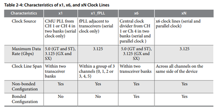
As a possible workaround, you may consider using fPLL(s) to drive the remaining channels. However, whether this approach is supported and can be successfully placed depends on the specific design constraints and routing availability. In this scenario, two fPLLs would be required (1 for bottom 3 channels and another for top 3 channels).
To determine feasibility, I recommend creating a simple test design and running it through a Quartus Fitter compilation to verify whether the placement and routing can be successfully achieved.
Please let me know if you have any concerns or need further clarification.
Thank you.
 Contributor
A bit hard to understand on:
"However, whether this approach is supported and can be successfully placed depends on the specific design constraints and routing availability. In this scenario, it is likely that two fPLLs would be required (1 for bottom 3 channels and another for top 3 channels), but this cannot be confirmed upfront."
What do you mean constraint so you do mean there is constraint that can force or make it routable?
And what do you mean routing availability?
Two fPLLs is due to what bases and how about the x1 xN configuration?
The device had been years over decade aren't these configuration possibilities are very well documented?
Thanks,
Brian

