 New Contributor
Cyclone IV GX transceiver kit clocking (documentation) confusion
I am going through the shit documentation and this is confusing me a lot. Someone please help me get through this mess.
Question 1: Where is the 50MHz clock (what pin)?
Question 2: Where is the switch to select the 125MHz clock?
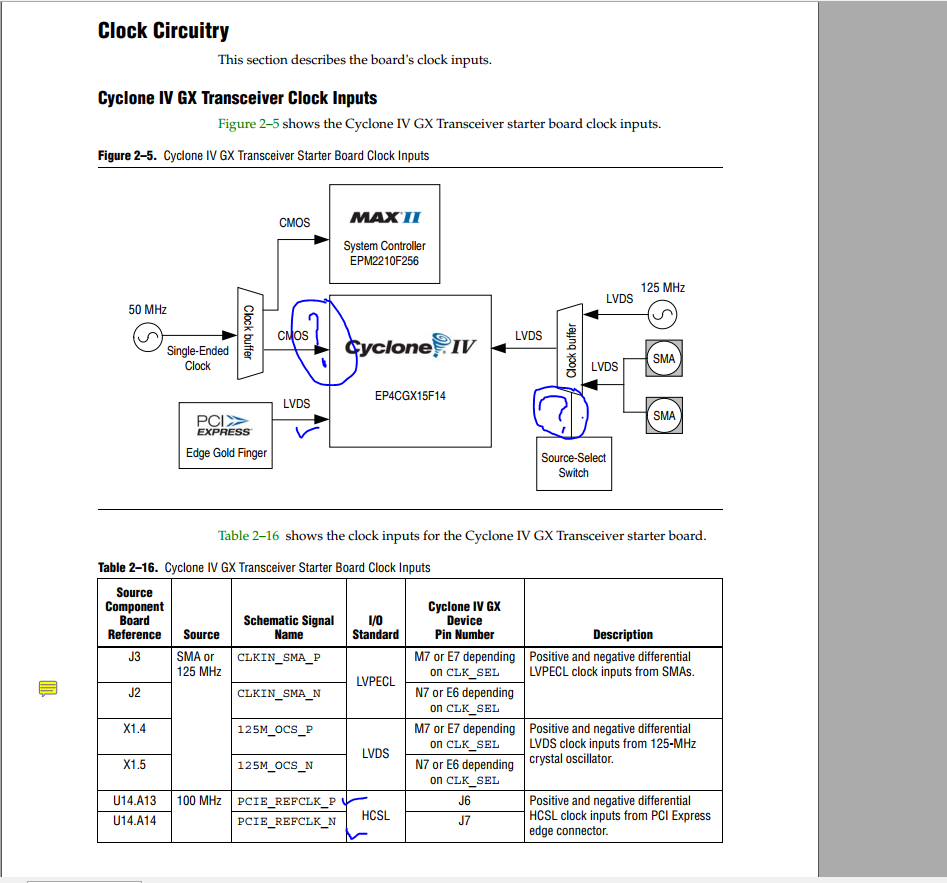
Please see attached image to understand why I'm getting confused.
---------------------------------------------------------------
Image1 : clocking_cycloneIVgx_transceiverkit
---------------------------------------------------------------
clearly there are 3 clock inputs:
clock input 1: 100MHz from PCIE (no confusion ; I also have pin number)
clock input 2: 50MHz clock show in image, but not in table 2-16 (where is this?)
clock input 3: 125MHz/SMA clock depending in CLK_SEL (okay...but where the hell is CLK_SEL?) Image 2 is related to this point.
---------------------------------------------------------------
Image 2 : dip_shit(switch)
---------------------------------------------------------------
There is supposed to be a physical switch on the board to help me select between SMA and on-board 125 MHz clock. Where is this switch???
Image 3 is related to this point
---------------------------------------------------------------
Image 3 : sma_clock_input
---------------------------------------------------------------
Where is this switch they are talking about? I removed the LCD panel. There ain't no switch?!?!?!
---------------------------------------------------------------
Image 3 : 50MHz_clock
---------------------------------------------------------------
Where is the 50-MHz clock??
Where is the CLK_SEL?
I'm even attaching the manual for your reference (and also as a sanity check that I'm not missing anything)
Really appreciate the time taken to sort this mess. How do they(intel/altera) expect someone to learn when there is lot of confusion in the documentation itself....is something that amazes me....anyways...any help appreciated


.PNG)