Forum Discussion

 Occasional Contributor
Cyclone 10 GX AS x4 Configuration Compatibility with Infineon S25FS512S (Custom Flash Definition)
 Occasional Contributor
Hello Fabri,
Update on AS x4 configuration debugging
I performed the following tests with the Cyclone 10 GX and Infineon S25FS512S:
1. Quad I/O dummy clock = 10, Single I/O dummy clock = 8
The FPGA image did not configure successfully in AS x4 mode.
2. Quad I/O dummy clock = 8, Single I/O dummy clock = 8
The FPGA image still did not configure successfully in AS x4 mode.
3. Manual JIC data-shifting experiment
I then investigated the suggested data-alignment compensation by modifying the JIC image data. Before making the modification, I analyzed the beginning of the JIC file. The region from approximately 0x00000000 to 0x000000AA contains JIC metadata, including Quartus Prime Programmer/version information and flash/device-related information. Therefore, I preserved this region and did not apply the data shift to this metadata.
I then attempted to shift the relevant image data by two bytes based on the observed AS x4 read sequence. However, when I tried to program the modified JIC file, Quartus Programmer reported that the image was corrupted.
Saleae capture observation
While analyzing the AS x4 configuration sequence using a Saleae logic analyzer, I observed that the FPGA does not immediately start the configuration image read using EBh.
Initial access:
9Fh (Read Device ID)
↓
0Bh (Single I/O Fast Read)
Address = 0x00040000
↓
Later:
EBh (Quad I/O Read)
Address = 0x000403B8
↓
Configuration does not complete
↓
9Fh (Read Device ID) is issued again
↓
Access returns to approximately:
0x00040000
0x000403B8
↓
Sequence repeats
In my case, the EBh access occurs at an offset of:
0x000403B8 - 0x00040000 = 0x3B8
So I would like to understand the purpose of the 0x3B8 offset and the reason for the initial 0Bh read before the subsequent EBh access.
Based on the previous discussion regarding the two-clock difference between the Cyclone 10 GX AS x4 controller and the flash, I investigated whether data alignment at this location could be the cause. However, manually shifting the JIC data resulted in a corrupted JIC file.
Could you please clarify:
Is the initial 0Bh read followed by an EBh read at image base + 0x3B8 an expected Cyclone 10 GX AS x4 configuration sequence?
What is the purpose of the 0x3B8 offset?
Where exactly should the two-clock (+2) compensation be applied?
Should the compensation be handled entirely by Convert Programming File, rather than by manually modifying the JIC image?
Is there any additional requirement for the S25FS512S mode byte or dummy-cycle configuration for Cyclone 10 GX AS x4?
Thanks
Sumanth Srinivas

 Regular Contributor
Hello Sumanth,
CR2NV / CR2V register breakdown as below:
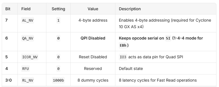
Why Bit 6 Must Remain 0
1. Cyclone 10 GX Active Serial (AS x4) Uses the 1-4-4 Protocol
During AS x4 configuration, the Cyclone 10 GX configuration controller acts as the SPI master and issues the Fast Read Quad I/O (EBh) command:
- Instruction (Opcode EBh): Transmitted serially on 1 line (DATA0/SI) over 8 clock cycles.
- Address: Transmitted on 4 lines (DATA[3:0]) over 8 clock cycles (for 32-bit / 4-byte addressing).
- Mode / Latency (Dummy Cycles): Transmitted/waited on 4 lines (DATA[3:0]).
- Data Output: Read on 4 lines (DATA[3:0]).
This is strictly an Extended SPI 1-4-4 protocol. The Cyclone 10 GX hard configuration control block does not support QPI (4-4-4 protocol) during device power-up configuration.
2. What Happens if Bit 6 is Set to 1 (0xC8)
As shown in Table 26 (Configuration Register 2 Non-volatile):
- Bit 6 (QA_NV):
- 0 = Disabled: Legacy SPI protocols in use; instructions are always serial on SI (1-x-x protocols supported).
- 1 = Enabled: QPI (4-4-4) protocol in use; all instructions (including opcodes) must be driven on all 4 lines (IO[3:0]).
If bit 6 is set to 1 (0xC8):
- Upon power-up, the flash enters QPI mode and expects opcodes to arrive as 4-bit nibbles across IO[3:0] over 2 clock cycles.
- The Cyclone 10 GX drives the EBh opcode serially on DATA0 only over 8 clock cycles while DATA[3:1] remain undriven (or pulled high).
- The flash reads all 4 data lines simultaneously, receives an unrecognized opcode, and fails to decode the command.
- Consequently, no configuration bitstream is returned, CONF_DONE never transitions high, and configuration fails.
Notes: A common point of confusion is between Quad Operation Enable and QPI Protocol:
- Quad Enable (CR1V[1] / CR1NV[1] = 1): Required for AS x4. It enables the IO3/RESET# and IO2 pins for quad data transactions and permits quad read commands like EBh (1-4-4), while keeping opcode entry serial (1-line).
- QPI Enable (CR2NV[6] = 1): Forces the instruction/opcode phase itself to be 4-line (4-4-4). This is incompatible with Cyclone 10 GX AS x4.
This setting aligns with Altera AN 1013 (Using Generic QSPI Flash on Control Block-Based Devices, Section 6.1), which specifies the 4-byte register initialization write (0x01 command) for Cypress/Infineon flashes configured with Cyclone 10 GX AS x4 as: Data=0x00 0x02 0x88 0x08\text{Data} = \texttt{0x00 0x02 0x88 0x08}Data=0x00 0x02 0x88 0x08 where the 3rd byte (CR2) is explicitly configured to 0x88.


