Forum Discussion

 Occasional Contributor
Cyclone 10 GX AS x4 Configuration Compatibility with Infineon S25FS512S (Custom Flash Definition)
 Occasional Contributor
Hello Fabri,
Update on AS x4 configuration debugging
I performed the following tests with the Cyclone 10 GX and Infineon S25FS512S:
1. Quad I/O dummy clock = 10, Single I/O dummy clock = 8
The FPGA image did not configure successfully in AS x4 mode.
2. Quad I/O dummy clock = 8, Single I/O dummy clock = 8
The FPGA image still did not configure successfully in AS x4 mode.
3. Manual JIC data-shifting experiment
I then investigated the suggested data-alignment compensation by modifying the JIC image data. Before making the modification, I analyzed the beginning of the JIC file. The region from approximately 0x00000000 to 0x000000AA contains JIC metadata, including Quartus Prime Programmer/version information and flash/device-related information. Therefore, I preserved this region and did not apply the data shift to this metadata.
I then attempted to shift the relevant image data by two bytes based on the observed AS x4 read sequence. However, when I tried to program the modified JIC file, Quartus Programmer reported that the image was corrupted.
Saleae capture observation
While analyzing the AS x4 configuration sequence using a Saleae logic analyzer, I observed that the FPGA does not immediately start the configuration image read using EBh.
Initial access:
9Fh (Read Device ID)
↓
0Bh (Single I/O Fast Read)
Address = 0x00040000
↓
Later:
EBh (Quad I/O Read)
Address = 0x000403B8
↓
Configuration does not complete
↓
9Fh (Read Device ID) is issued again
↓
Access returns to approximately:
0x00040000
0x000403B8
↓
Sequence repeats
In my case, the EBh access occurs at an offset of:
0x000403B8 - 0x00040000 = 0x3B8
So I would like to understand the purpose of the 0x3B8 offset and the reason for the initial 0Bh read before the subsequent EBh access.
Based on the previous discussion regarding the two-clock difference between the Cyclone 10 GX AS x4 controller and the flash, I investigated whether data alignment at this location could be the cause. However, manually shifting the JIC data resulted in a corrupted JIC file.
Could you please clarify:
Is the initial 0Bh read followed by an EBh read at image base + 0x3B8 an expected Cyclone 10 GX AS x4 configuration sequence?
What is the purpose of the 0x3B8 offset?
Where exactly should the two-clock (+2) compensation be applied?
Should the compensation be handled entirely by Convert Programming File, rather than by manually modifying the JIC image?
Is there any additional requirement for the S25FS512S mode byte or dummy-cycle configuration for Cyclone 10 GX AS x4?
Thanks
Sumanth Srinivas
 Farabi_Altera13 days ago
Regular Contributor
Hi Sumanth, This is a detailed and well-instrumented debug report — let me address each of your questions based on what's documented for the Cyclone 10 GX AS configuration controller.
1. Is the 0Bh → EBh sequence (with EBh at base + 0x3B8) expected?
The documented AS x4 configuration sequence for Cyclone 10 GX does begin with a device ID read (9Fh / RDID), followed by a single-I/O fast read (0Bh) to read boot/header information from the flash, before switching to the quad I/O fast read (EBh) for the main configuration data stream. This is expected behavior — the controller uses the initial 0Bh read to parse the configuration header stored at the base address, which tells it where the actual bitstream begins and what mode to use. The EBh access then starts at the bitstream payload offset rather than at address 0x0.
The 0x3B8 offset you observed (0x000403B8 − 0x00040000) is consistent with this: the JIC image stores a header/metadata block at the beginning of the flash partition, and the AS controller reads through it in single-I/O mode before jumping to the bitstream start address for quad-I/O streaming. The exact size of that header region can vary with Quartus Prime version and device density, but an offset of a few hundred bytes is normal. The fact that the sequence repeats (9Fh → 0Bh → EBh → fail → 9Fh again) is the controller's retry behavior after a configuration failure — it is not looping because the address is wrong, but because the EBh read is returning data the controller cannot validate.
2. Root cause: dummy cycle mismatch for the S25FS512S (Infineon/Cypress)
AS configuration failure with Cypress/Infineon S25FSxxxS flash occurs when the flash configuration registers are not set correctly. For AS x4 (quad) configuration with the S25FSxxxS, the flash configuration registers (CR2NV/CR2V) must be set to 0xC8 before configuration starts — this encodes: AS×4 scheme, 4-byte addressing, and 8 dummy clock cycles. Why does Active Serial (AS) configuration fail with Cypress® flash S25FSxxxS in Intel® Arria® 10 devices and Intel® Cyclone® 10 GX?
Your test #2 used Quad I/O dummy = 8, which matches the 0xC8 requirement on the dummy-cycle side — but the key question is whether CR2NV/CR2V on the physical flash device was actually programmed to 0xC8 before the FPGA attempted to configure. The Cyclone 10 GX AS controller issues the EBh command with a fixed dummy-cycle count; it does not negotiate with the flash. If the flash's non-volatile register (CR2NV) still holds its factory default (which is typically not 0xC8), the flash will respond with garbage data regardless of what dummy count you set in Quartus.
Action required: Use an external processor, a JTAG-based flash programmer, or a pre-programming step to explicitly write CR2NV = 0xC8 to the S25FS512S before the FPGA configuration attempt. This is a one-time NV register write to the flash device itself, separate from the JIC programming step.
Additionally, the Programming Object File (.pof) or Raw Programming Data (.rpd) should be generated with the 'Disable EPCS/EPCQ ID check' option enabled Why does Active Serial (AS) configuration fail with Cypress® flash S25FSxxxS in Intel® Arria® 10 devices and Intel® Cyclone® 10 GX? , since the S25FS512S is not an Altera EPCQL device and its JEDEC ID will not match the expected value.
3. The two-clock compensation and JIC data shifting
Do not manually shift JIC image data. The JIC file has a structured format with CRC fields and metadata that Quartus Programmer validates — any manual byte-level edit will corrupt the file integrity check, exactly as you observed. The dummy-cycle compensation is handled at the hardware protocol level (the flash's CR2NV register setting), not by offsetting the bitstream payload in the JIC. The Convert Programming File tool generates the correct bitstream layout; the flash register must be configured to match what the AS controller expects.
4. Flash addressing requirement
Cyclone 10 GX devices only support 4-byte addressing and 10 dummy clock cycles for single I/O fast read commands (0Bh), and the AS controller is fixed to these parameters. Customizable Flash Programmer User Guide If your flash device does not support power-up 4-byte addressing mode, it cannot be used for Cyclone 10 GX configuration. Customizable Flash Programmer User Guide The S25FS512S does support 4-byte addressing, but again, CR2NV must be set to enable it in the correct mode.
Summary checklist for S25FS512S + Cyclone 10 GX AS×4:
1-Program CR2NV = 0xC8 on the flash (4-byte addressing, 8 dummy cycles for quad, AS×4 scheme) using an external host before FPGA configuration.
2-Generate your .pof/.rpd/.jic with 'Disable EPCS/EPCQ ID check' enabled in Convert Programming File.
3-Do not manually modify JIC binary data — let Quartus Prime generate the correct file.
4-Confirm the flash is in 4-byte address mode at power-up (check CR2NV, not just CR2V which is volatile).
The repeating 9Fh/0Bh/EBh sequence you captured is the retry loop — once the flash register is correctly set and the ID check is disabled, the EBh read at base+0x3B8 should return valid bitstream data and configuration should complete.
- Farabi_Altera12 days ago
Hi Sumanth, do you have further question?
- Farabi_Altera1 hour ago
Hello Sumanth,
CR2NV / CR2V register breakdown as below:
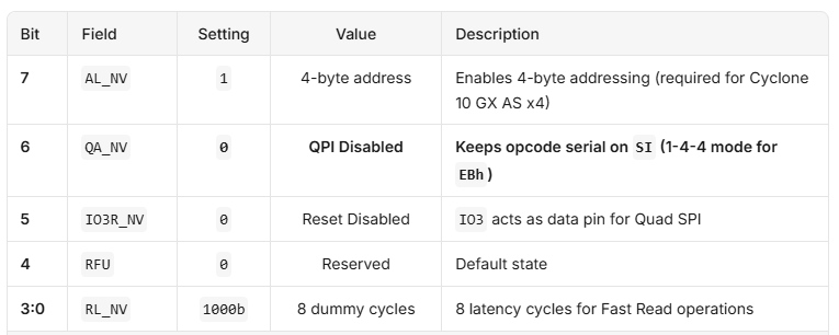
Why Bit 6 Must Remain 01. Cyclone 10 GX Active Serial (AS x4) Uses the 1-4-4 Protocol
During AS x4 configuration, the Cyclone 10 GX configuration controller acts as the SPI master and issues the Fast Read Quad I/O (EBh) command:
- Instruction (Opcode EBh): Transmitted serially on 1 line (DATA0/SI) over 8 clock cycles.
- Address: Transmitted on 4 lines (DATA[3:0]) over 8 clock cycles (for 32-bit / 4-byte addressing).
- Mode / Latency (Dummy Cycles): Transmitted/waited on 4 lines (DATA[3:0]).
- Data Output: Read on 4 lines (DATA[3:0]).
This is strictly an Extended SPI 1-4-4 protocol. The Cyclone 10 GX hard configuration control block does not support QPI (4-4-4 protocol) during device power-up configuration.
2. What Happens if Bit 6 is Set to 1 (0xC8)
As shown in Table 26 (Configuration Register 2 Non-volatile):
- Bit 6 (QA_NV):
- 0 = Disabled: Legacy SPI protocols in use; instructions are always serial on SI (1-x-x protocols supported).
- 1 = Enabled: QPI (4-4-4) protocol in use; all instructions (including opcodes) must be driven on all 4 lines (IO[3:0]).
If bit 6 is set to 1 (0xC8):
- Upon power-up, the flash enters QPI mode and expects opcodes to arrive as 4-bit nibbles across IO[3:0] over 2 clock cycles.
- The Cyclone 10 GX drives the EBh opcode serially on DATA0 only over 8 clock cycles while DATA[3:1] remain undriven (or pulled high).
- The flash reads all 4 data lines simultaneously, receives an unrecognized opcode, and fails to decode the command.
- Consequently, no configuration bitstream is returned, CONF_DONE never transitions high, and configuration fails.
Notes: A common point of confusion is between Quad Operation Enable and QPI Protocol:
- Quad Enable (CR1V[1] / CR1NV[1] = 1): Required for AS x4. It enables the IO3/RESET# and IO2 pins for quad data transactions and permits quad read commands like EBh (1-4-4), while keeping opcode entry serial (1-line).
- QPI Enable (CR2NV[6] = 1): Forces the instruction/opcode phase itself to be 4-line (4-4-4). This is incompatible with Cyclone 10 GX AS x4.
This setting aligns with Altera AN 1013 (Using Generic QSPI Flash on Control Block-Based Devices, Section 6.1), which specifies the 4-byte register initialization write (0x01 command) for Cypress/Infineon flashes configured with Cyclone 10 GX AS x4 as: Data=0x00 0x02 0x88 0x08\text{Data} = \texttt{0x00 0x02 0x88 0x08}Data=0x00 0x02 0x88 0x08 where the 3rd byte (CR2) is explicitly configured to 0x88.


