Forum Discussion

Altera_Forum Honored Contributor
17 years agoHonored ContributorSRAM K1B3216B2E on Cyclone III Development Kit
dear sopc experts,
has anyone used the 2 x 32mbit sram K1B3216B2E on altera cyclone III development kit or altera stratix III development kit? my problem: i instantiated a sopc with an tristate bridge, where my sram-interface is the mm-slave. my sram-interface component is associated with the SRAMInterface.vhd. can anybody tell me, what i've done wrong? because it doesn't work! thanks in advance! reto33 Replies
 Altera_Forum
According to the datasheet its a 70ns memory, when used asynchronously. It's not a real SRAM, but a DRAM with a SRAM-like interface.
If you need more performance you can use it in synchronous mode and access it in bursts, but you would need to write your own controller.- Altera_Forum
hello i have this same problem like you had with utram on cyclon iii ep3c120 dsp kit. i want to start working with this kit using utram. I try to use yours sopcbuilber component but it does not work in my case. please send me how to find solution of this problem.
regards Marcin - Altera_Forum--- Quote Start --- hello i have this same problem like you had with utram on cyclon iii ep3c120 dsp kit. i want to start working with this kit using utram. I try to use yours sopcbuilber component but it does not work in my case. please send me how to find solution of this problem. regards Marcin --- Quote End --- Send me a mail, and I will send you an example running on the kit (sram, ddr2ram and flash). m.hellmanns (at) tu-bs.de
- Altera_Forum--- Quote Start --- Send me a mail, and I will send you an example running on the kit (sram, ddr2ram and flash). m.hellmanns (at) tu-bs.de --- Quote End --- Hello i want to use that utram component but there is only one wait signal on it. Memory on ep3 dsp kit have two. How i should connect them. What clock and timing settings i should make? How i should connect address signal? I have 50MHz sys clock and sram clock. Regards Marcin.
- Altera_Forum
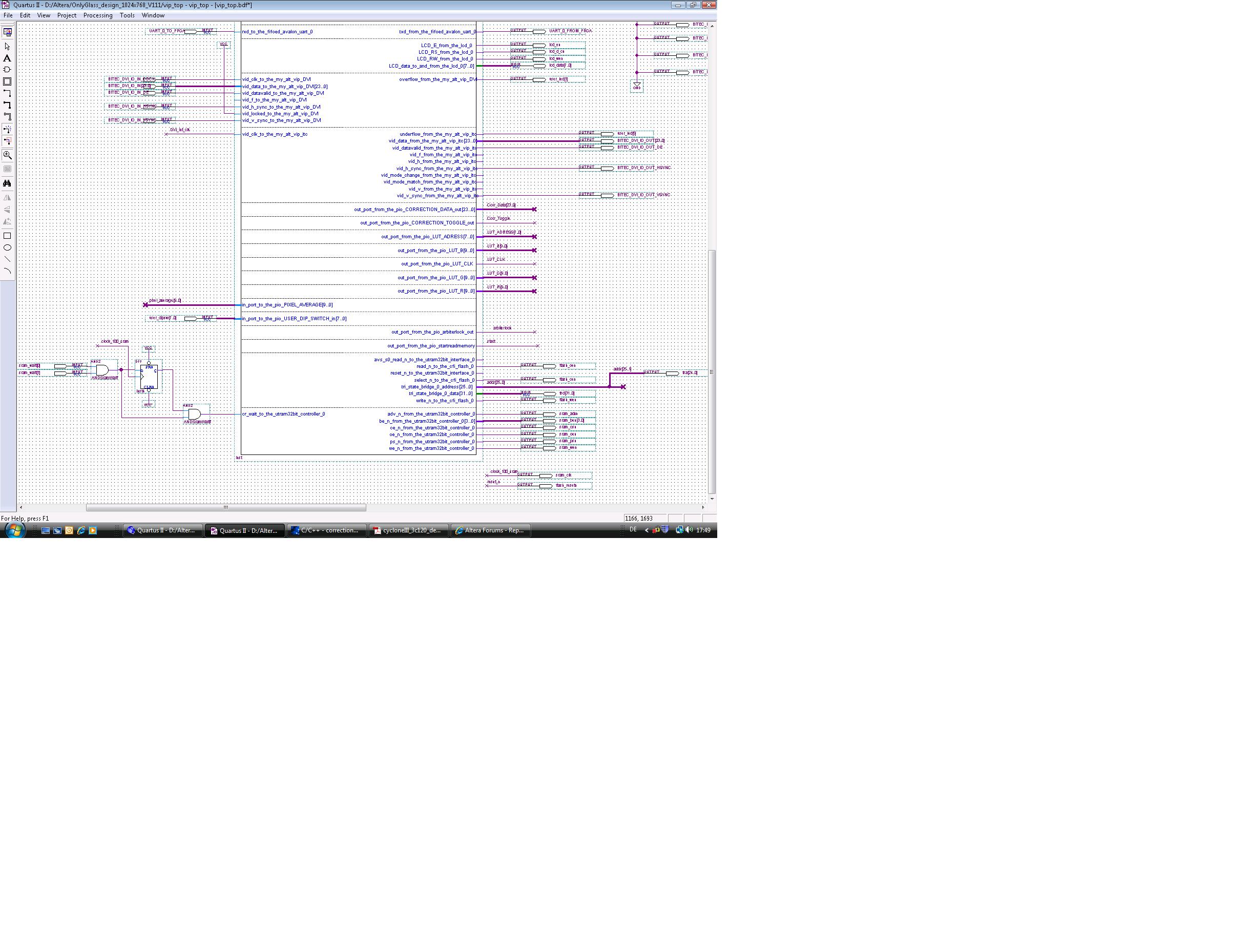
Please use an and-logic and a latch for the wait-signal.
Remember the lsb of the tristate address is not connected (tristate bus: 26 bit (25..0), sram and flash bus: 25 bit (24..0). Timing: Use a pll to generate the 100MHz clock for the avalon bus in SOPC-builder. Generate another 100MHz clock for the SRAM with a phase shift of -3,5ns The utram is optimised for 100MHz clock. See the documentation in the \ip\utram directory for other timings. see attachment for wait-logic and assigning the address-bus. - Altera_Forum--- Quote Start --- Please use an and-logic and a latch for the wait-signal. Remember the lsb of the tristate address is not connected (tristate bus: 26 bit (25..0), sram and flash bus: 25 bit (24..0). Timing: Use a pll to generate the 100MHz clock for the avalon bus in SOPC-builder. Generate another 100MHz clock for the SRAM with a phase shift of -3,5ns The utram is optimised for 100MHz clock. See the documentation in the \ip\utram directory for other timings. see attachment for wait-logic and assigning the address-bus. --- Quote End --- thanks for your quick reply. thet example pass memory test as well but i still do not have working project. I tried to extract utram component and put it to my project but my nios can not run using that memory. Do you have idea what is wrong . Regards Marcin
- Altera_Forum--- Quote Start --- thanks for your quick reply. thet example pass memory test as well but i still do not have working project. I tried to extract utram component and put it to my project but my nios can not run using that memory. Do you have idea what is wrong . Regards Marcin --- Quote End --- Did you check running Nios from Onchipram and accessing the utram from nios?
- Altera_Forum--- Quote Start --- thanks for your quick reply. thet example pass memory test as well but i still do not have working project. I tried to extract utram component and put it to my project but my nios can not run using that memory. Do you have idea what is wrong . Regards Marcin --- Quote End --- You have mapped the tristate addressbus which reaches from 22..0 to 22..1 (the first lsb isn't used). That's right. But then you assigned the sram from 22..1 to this bus. That't incorrect. You have to assign the sram from 21..0 to this bus. the reason: the sram addressbus starts with FSA1. so you might think you have to left out FSA0 - but if you use flash you need the FSA0 and so the editor of the utram-interface considers that.
- Altera_Forum
I still working and i have no solution. i still dont now what mistake i do.
If you have some idea please help me. This referens design is working as well at quartus 9.1, but my own project at quartus 7.2 is not working well. - Altera_Forum--- Quote Start --- I still working and i have no solution. i still dont now what mistake i do. If you have some idea please help me. This referens design is working as well at quartus 9.1, but my own project at quartus 7.2 is not working well. --- Quote End --- Is not working well? What does that mean? Can you load a design into onchip mem and then read/write to the sram? if not: Please send a new picture of SOPC builder and of the block-diagramm. Check your pin-assignment (the name,the location, the io-standard). If you don't now, compare the pin-assignment of the running example with yours. If this doesn't lead to success, mail me your archieved project file, and I'll have a look.