hps arch
33 Topics
Introducing the Altera Community AI Responder — Beta
Altera is introducing the AI Responder, an assistant built into the Altera Community to help provide faster, context-aware guidance for Altera product questions. It uses relevant public Altera documentation and Knowledge Database content, with coverage continuing to expand. The AI Responder may provide source references and can hand off complex or out-of-scope questions to an Altera subject-matter expert. As a beta feature, responses may contain errors or omissions, so please review the sources and verify technical guidance against official Altera documentation before implementation. If the response does not fully address your question, add more context and tag ai_responder to continue the discussion. We welcome your feedback as we improve the Community experience.19Views0likes0Comments
LWH2F Throughput
Dear all, I'm facing the issue that the throughput on the Agilex 5 LWH2F interface appears to be lower compared to Cyclone 5. - I have two custom boards, one is based on Cyclone 5, the other on Agilex 5. - I use a linux OS. The code runs in a linux kernel driver. The code for the driver is the same for both devices. - The memory is mapped using ioremap(), i.e. it is mapped as device memory. - I measure performance by taking a timestamp with ktime_get_ns(), then read/write 10000 uint32 values, then take another timestamp. - I've measured the follwing values - Cyclone5 board read: 47.2 MB/s (million bytes per second or 11.8 million words à 4 byte per second) - Cyclone5 board write: 73.1 MB/s - Agilex5 board read: 24.8 MB/s - Agilex5 board write: 18.8 MB/s - I've noticed that performance varies, depending on the CPU that the process is running on (when measuring in userspace I can explicitly set the cpu affinity; For the kernel driver I've noticed that it is sometimes slower than above, presumably because it's running on a different cpu). - There is a slight difference in the QSYS design: - The Cyclone5 based board: - drives the AXI bus with a 64 MHz clock. - uses the Avalon MM Slave Translator. - The Agilex5 based board: - drives the AXI bus with a 200 MHz clock. - uses the Avalon Memory Mapped Pipeline Bridge Intel FPGA IP. - Our FPGA takes one 64/200 MHz cycle to process the read (readdatavalid). For a write our FPGA doesn't generate a writeresponsevalid, this is handled by the IP block. - I'm using Quartus 25.1.1 for the Agilex 5 design. I'm aware that the LWH2F interface is not intended for high throughput. Also, since the memory is mapped as "Device Memory", every load/store is processed separately and we're not taking advantage of AXI bursts, etc. I'm aware that we could improve performance by using the H2F interface and mapping the memory as normal memory. That said, we have a prooven design and are reluctant to change it unless absolutely neccessary. So I have the following questions: - Is a higher latency expected on Agilex5? (E.g. due to a different architecture of the interconnect) - Have you measured the performance of the LWH2F interface? Can you give me a number on how many transactions per second we can expect? Kind Regards, Eric Opitz488Views0likes13Comments
Release 26.1.1
Version: Release 26.1.1 PRO Quartus Build/TAG: B130/QPDS26.1.1_REL_GSRD_PR Release Date: August 17, 2026 Device Affected: Agilex™ 3, Agilex™ 5, Agilex™ 7, Startix® 10 Release Type: Major release/Binary release Binary Release Path: http://releases.rocketboards.org/2026.08/ Release Page: https://github.com/altera-fpga/gsrd-socfpga/releases/tag/QPDS26.1.1_REL_GSRD_PR Major Features Released Agilex™ 5 XEN Hypervisor 5 System Example Design https://altera-fpga.github.io/rel-26.1.1/virtualization/hypervisors/xen/ug-xen-agx5e-premium-065b/ , https://altera-fpga.github.io/rel-26.1.1/virtualization/hypervisors/xen/ug-xen-agx5e-premium-065a/ Agilex™ 5 RYO OPTE System Example Design Agilex™ 5 Quartus Reference Design using VDS Agilex™ 3 Time-Sensitive Networking (TSN): PHY configuration 2 (RGMII from FPGA HVIO) System Example Design Agilex™ 5 Performance Optimized Baseline SED support Agilex™ 5 DataMover / Bridge and Memory Benchmark System Example Design https://altera-fpga.github.io/rel-26.1.1/embedded-designs/agilex-5/e-series/premium-065a/data-mover/ug-data-mover-agx5e-premium-065a/ Agilex™ 3 support of FreeRTOS Agilex™ 5 Terasic DE25-Nano Board System Example Design103Views2likes0CommentsHow to Generate Altera HAL for HPS?
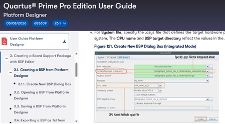
Hi, I am using Quartus 26.1 with the Agilex 5 Modular Development Kit (Device number: A5ED065BB32AE6SR0) and I have a few questions about BSP Generation for Hard Processor System (HPS). For reference I am following the Quartus Prime Pro Edition Version 26.1 User Guide. 1. How do I generate Altera HAL for HPS? When I use the BSP Editor in platform designer, I can only generate the system.h file that only has macros for EMIF, even though other peripherals are also connected to the HPS. How do I generate macros for the H2F bridges and HAL API Files for the HPS? 2. How do I input a SOPCINFO file into the BSP Editor? The Quartus Prime Pro Edition User Guide shows that I should be able to input SOPCINFO file as the system file (see above image) but Quartus only gives me the options of QSYS and IP file (see below image). Thank you for the help!Solved247Views0likes5Comments
Agilex 5E HPS and Linux
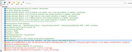
Hi. 1. Is there a simple method to run two Linux systems on HPS, i.e.: Linux 1 - 2xA55 and Linux 2 - 2xA76 with different sets of peripherals? 2. Is it possible to use one Ethernet port by these two Linux systems. 3. Is there a simple method for communication between these two Linux systems?567Views0likes8CommentsF2SDRAM fails to synthesize with custom logic
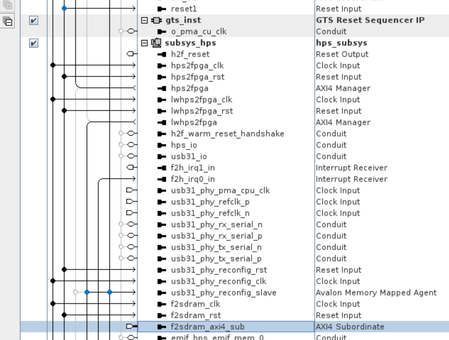
Hello guys, We are using Agilex5 SOC F2SDRAM bridge. I am trying to connect custom logic to the F2SDRAM, but it absolutely refuses to synthesize unless I export the signals directly to the top-level ports. Does anyone know why this is happening? Also, is there an example design for F2SDRAM available? The GHRD is not very helpful since it only includes the JTAG master. I suspect it might be a design issue, so I even removed the adapter and connected it only within Qsys, but it’s still acting up like this. Does anyone know why this is happening even though everything is clearly declared and connected? HudsonSolved537Views0likes20CommentsF2SDRAM test inquiries.
Hi Guys, I am testing the F2SDRAM bridge. 32 bit address, 256bits data. Due to recurring missing Verilog file errors for the Qsys adapter IP whenever switching PCs, I removed the adapter earlier and am currently testing by directly exporting f2s from the HPS to the top level. I implemented tester logic on the FPGA side to write and read 256-bit data once per transaction (len=0) for 2048 comparisons, but the B channel signal keeps returning 2'b11 (DECERR). I implemented the tester logic on the FPGA side to perform 2,048 read/write comparison cycles with 256-bit data in single-beat transactions (len=0) using a base address of 0x8000_0000. However, I am at a loss because the B channel signal continuously returns 2'b11 (DECERR). Debugging this solely based on the B channel response is quite challenging. For reference, I am currently running this test on an 013b devkit using the GHRD Linux Reference Design, triggering the start signal via Signal Probe after the kernel has fully booted up Could this be an issue with sideband signals or the kernel driver? Gemini suggests that the bridge might be in reset or it could be due to SMMU. I have already disabled SMMU. As expected, learning and applying new technology is always tough. Thank.Solved220Views0likes6CommentsStratix 10 Linux SD card booting
Hi Altera Community, I tried multiple attempts to boot the SD card from Rocketboard.org. https://releases.rocketboards.org/ I downloaded and booted the SD card with the .wic image file. It only has the .itb file by default in the boot partition. Whenever I try to boot, it asks for the U-Boot.img file. And also it says "failed to load "socfpga_stratix10_socdk.dtb" even if the file is there. And then I compiled my simple HPS design and can easily program the FPGA from the Quartus Programmer (rbf and sof file), but whenever I try to overlay it, like say: echo overlay.dtb > /sys/kernel?config?device-tree/overlays/0/path It says "FPGA manager error, timeout," and so on. Does any community member have notes or steps that you made to boot the SD card of the Stratix 10 FPGA? I am following this link: https://www.rocketboards.org/foswiki/Documentation/BuildingBootloaderStratix10249Views0likes11Comments
TSE -> SGDMA -> SOC(through f2sdram)
Hi, I'm trying to transfer an old design with multiple TSEs / SGMDAs and a NIOS to a newer Agilex 5. We are also evaluating the use of the SOC instead of the NIOS in the design. I've made a minimized platform design for it but it fails during synthesis with the notorious error for the f2sdram bus: There is both a 'memory -> streaming' and 'streaming -> memory' sgdma in the design present, so both read and write port on the axi bus should be present. If I connect the SGDMA's to the fpga2hps bus the same error is generated. Are there settings in the SGDMAs that needs to be set to a certain value so that the correct read/write avalon MM/AXI interface is generated?174Views0likes4Comments