arria® 10 fpgas and socs
1380 Topics
Why Can't I Program Using Active Serial Programming with my USB Blaster III?
Description Due to a firmware issue the USB Blaster III Development cable may not have the correct product ID and may inadvertently disabled FLASH programming using the active serial x1/x2 interface in the Quartus Programmer. It does not impact just using ASx4 to program your FPGA or using JTAG to program your flash device. Is my Development Cable affected by this? If your USB Blaster III Development cable has a serial number ranging from UB3000000 - UB3006090, then you will need to update the PID. Resolution To resolve this issue the Product ID of the cable should be updated to (6023). Perform the following steps on Windows to update the ID. Download and Install the FT_PROG.exe the EEPROM Programming Utility from FTDI https://ftdichip.com/utilities/ Plug-in your USB Blaster III development cable into your computer. Uninstall the USB Blaster III device driver from the device manager. Open the Windows Device Manager. Find the group called JTAG cables, under this group there should be a USB Blaster III device. Right Click on the USB Blaster III device and Click Uninstall. Tick "Attempt to delete the driver for this device" or "Delete the driver software for this device" during uninstallation. This prevents the UB3 driver from being automatically reinstalled. Install the FTDI Device driver. Open the Windows Device Manager. Find the group called Other Devices. In the group Other Devices there may be several USB Blaster III devices. To Identify the correct USB Blaster III device Right click on each USB Blaster III device and click Properties. Find USB Blaster III device that contains values that end with MI_00 Once Identified, Right click on correct USB Blaster III device and click Update driver To Update driver click Browse my computer for drivers Search and select the USB Blaster III driver directory under your Quartus installation. <Quartus Path>\qdrivers\quartus\drivers\usb-blaster-iii Click Let me pick from a list of available drivers on my computer. If, Select your device’s type from the list below, choose Universal Serial Bus controllers. When selecting a driver click the FTDI manufacturer then select USB Serial Converter A Version: 2.12.36.4 and click the Next button. Program your USB Blaster III Development Cable with FT_PROG.exe to update your product ID. Open the FT_PROG.exe from FTDI installed in step 1. From the DEVICES menu click Scan and Parse to bring up your USB Blaster III Device Under the Device Tree select the section called USB Device Descriptor This should contain a property called Product ID and should have a value of 6023, change this to 6023 if it is not set to this value. Once changed, under the DEVICES menu click Program to flash the EEPROM Uninstall the FTDI driver installed in step 4. Open the Windows Device Manager. Find the group Universal Serial Sub controllers In the Universal Serial Bus controllers right click on the USB Serial Converter A and Click Uninstall. Do not tick "Attempt to delete the driver for this device" or "Delete the driver software for this device". Re-Install the USB Blaster III device driver. Open the Windows Device Manager. Find the group called Other Devices. In the group Other Devices there may be several USB Serial Port devices or USB Blaster III devices. To Identify the correct USB Serial Port device Right click on each USB Serial Port device and click Properties. Find USB Serial Port device that contains values that end with MI_00 Once Identified, Right click on correct USB Blaster III device and click Update driver To Update driver click Browse my computer for drivers Search and select the USB Blaster III driver directory under your Quartus installation. <Quartus Path>\qdrivers\quartus\drivers\usb-blaster-iii Click the Next button. Windows should show USB Blaster III driver installed. Verify USB Blaster III device has the correct Product ID. Open the Windows Device Manager. Find the group called JTAG cables, under this group there should be a USB Blaster III device. Right click on each USB Blaster III device and click Properties. Values should contain PID_6023 in the string, if not unplug and re-plugin the device. Open Quartus Programmer and Validate that the Active Serial programing is now available.531Views0likes0CommentsWhy does the SystemConsole.refreshMasters DSP Builder function fail?
Description When using the SystemConsole.refreshMasters DSP Builder function in the Quartus® Prime Pro Edition version 26.1.1 and above, you may see the following error: Unable to resolve the name 'com.altera.systemconsole.matlabapi.SystemConsoleLink' This error occurs because the Java version used by MATLAB is incompatible with com.altera.systemconsole.matlabapi.SystemConsoleLink. For DSP Builder version 26.1.1 and later, MATLAB must use Java version 11 or later for SystemConsole.refreshMasters to run successfully. Resolution You can change MATLAB's Java version using either the jenv MATLAB function or the matlab_jenv executable. For information on how to use jenv and matlab_jenv, refer to the MATLAB documentation.39Views0likes0CommentsWhy are there no example design options available in the “Select Design” drop-down list in the DisplayPort IP Parameter Editor GUI?
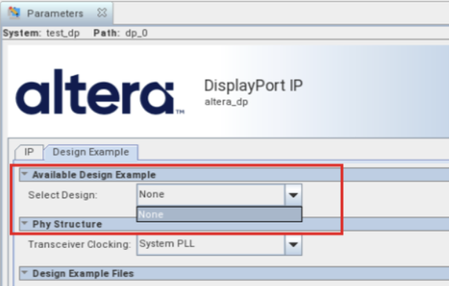
Description Due to a problem in the Quartus ® Prime Pro Edition Software version 26.1, the drop-down list for “Select Design” in the Display Port IP Parameter Editor GUI only has “None” option, as shown in the screenshot below. Resolution This problem has been fixed beginning with version 26.1.1 of the Quartus® Prime Pro Edition Software.166Views0likes0CommentsError: (vlog-7) Failed to open design unit file
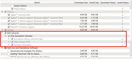
Description Due to simulation models not being installed along with the Quartus ® Prime Pro Edition Software, an error such as: Error: (vlog-7) Failed to open design unit file "C:/altera_pro/26.1.1/quartus/eda/sim_lib/220model.v" in read mode may occur during simulation. The root cause of missing files is that “EDA libraries” are not installed properly during installation of the Quartus ® Prime Pro Edition Software. Resolution To fix this problem, make sure “EDA Libraries” has been checked and installed properly during installation of the Quartus ® Prime Pro Edition Software, as shown in the screenshot below.94Views0likes0CommentsWhy am I unable to run BKP operations with Quartus® Prime Pro Edition 26.1.1 on Windows*?
Description Due to a problem in the Quartus® Prime Pro Edition Software version 26.1.1, Black Key Provisioning (BKP) operations might fail on Windows* with the following error: Error: BKP PLUGIN: [3000] Http error: Could not use specified SSL cipher because Quartus has enabled the Windows SSP interface Schannel (Secure Channel) to work with the OpenSSL library. When using libcurl with the Schannel (Windows) backend, the option CURLOPT_SSL_CIPHER_LIST does not accept individual, specific cipher suites (for example TLS_ECDHE_RSA_WITH_AES_256_GCM_SHA384). Resolution To work around this problem in the Quartus® Prime Pro Edition Software version 26.1.1, build a patched bkpprog.dll and select it through the project configuration, as follows: 1. Clone the source repository: GitHub - altera-fpga/device-security-software-services: Device Security Software and Services source code for FPGA Device Onboarding, Attestation, Secure Session, Black Key Provisioning. 2. Prepare the Windows build environment. Follow the Windows Build instructions in the repository README. Install the listed prerequisites and prepare the repository dependencies exactly as documented there. 3. Modify network_wrapper.cpp. Open the following file in the cloned repository: bkpprogrammer/src/core/cpp/network/network_wrapper.cpp In CurlWrapper::CurlWrapper, locate the TLS version and cipher-list configuration: setCurlOptionWithErrorHandling( curlHandle, CURLOPT_SSLVERSION, CURL_SSLVERSION_TLSv1_2); setCurlOptionWithErrorHandling( curlHandle, CURLOPT_SSL_CIPHER_LIST, acceptedCiphers.c_str()); Replace it with: setCurlOptionWithErrorHandling( curlHandle, CURLOPT_SSLVERSION, CURL_SSLVERSION_TLSv1_2); 4. Build the patched plug-in. Return to the repository root and build by following the repository Windows Build instructions. Confirm that bkpprog.dll is regenerated after network_wrapper.cpp was modified. 5. Place the custom plug-in. Create the following directory under the BKPS project and copy the rebuilt bkpprog.dll into it. Do not replace the DLL inside the Quartus installation. <project>\cm_provisioning\bkp_plugin\bkpprog.dll 6. Create quartus.ini. Create a quartus.ini file directly under the project cm_provisioning directory with the following line: PGM_ALLOW_CUSTOM_BKP_PLUGIN=7S6Nh0s3@on 7. Update bkp_options.txt. Use the normal project-specific BKP values and add bkp_plugin with the path to the rebuilt DLL: bkp_cfg_id = <ID> bkp_ip = <IP> bkp_port = <PORT> bkp_tls_ca_cert = "<Path_To_bkps_ssl_cert.crt>" bkp_tls_prog_cert = "<Path_To_pro_cert>" bkp_device_opn = <OPN> bkp_plugin = "<Path_To_bkpprog.dll>" 8. Run Quartus Programmer where quartus.ini is located. Set the current working directory to the cm_provisioning directory that contains quartus.ini and bkp_options.txt. Quartus reads quartus.ini from its current working directory, so run the commands from here: quartus_pgm.exe -c 1 -m jtag --bkp_options=bkp_options.txt --bkp_prefetch Use the same working directory for Set Authority and Provision operations, so Quartus continues to load the custom plug-in setting from quartus.ini. This problem is scheduled to be resolved in a future release of the Quartus® Prime Pro Edition Software.54Views0likes0CommentsWhy can’t I open the Early Power Estimator (EPE) tool in the latest version of Microsoft* Excel?
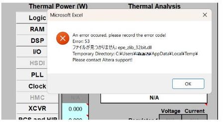
Description Due to the legacy design of the Early Power Estimator (EPE) worksheets, which include VBA macros, ActiveX components, and embedded DLL files, errors may occur when opening the Excel file on newer Windows platforms or when using Microsoft* Office 365, in both 32-bit and 64-bit versions. When the spreadsheet is opened, several actions occur in the background. Excel extracts the embedded DLLc files to the user's %TEMP% directory. A script then decompresses the DLLc files into standard DLL files. The script subsequently loads and executes the DLL files, which is used by the Excel macros. Why does this issue occur? To extract and execute the required DLL files, the Excel macros rely on a set of commands provided by Microsoft .NET and Microsoft Visual C++ runtime libraries, depending on the specific version of the Excel worksheet. In newer versions of Microsoft Windows and Microsoft Office 365, these runtime components are no longer bundled together by default, and some legacy functions used by older scripts have been deprecated or replaced with newer implementations. As a result, scripts designed for earlier environments may fail when attempting to call these functions. Note: In some systems, some of these are already installed automatically by other 3rd party software tools during installation. Additionally, the legacy script design does not support symbolic linking or modern handling of the user's %TEMP% directory, which can cause issues when extracting and accessing temporary files. Modern systems also enforce stricter security controls, including: ActiveX restrictions in newer versions of Microsoft Excel Trust Center policies that block code execution from untrusted locations Operating system security policies in Microsoft Windows that may prevent DLL execution from the %TEMP% directory if such restrictions are enabled As a result, if any of these conditions are triggered, users may encounter errors such as “Unable to find or load DLL files.” For example, errors may appear related to the zlib.dll file (the 32-bit or 64-bit version used depends on the installed Excel architecture). Resolution To workaround this issue PART A: Unblocking the Excel and Enable Macros/ActiveX 1. Unblock the Excel File • Right-click the EPE Excel file → Properties → Check Unblock under Security. • Click Apply → OK. 2. Enable Macros and ActiveX • Open Excel → File → Options → Trust Center → Trust Center Settings: Enable Macros. Enable ActiveX controls. Leave other settings as default (Safe Mode can remain enabled or disabled). 3. Check whether you can now open the EPE excel sheet. Else proceed to PART B. PART B: Installing the necessary Microsoft .NET and Visual C++ runtime libraries. Microsoft .NET installation Go to your Installed apps settings and find for .NET. It is recommended to have both .NET Runtime and ASP .NET installed in your system. If you already have a version installed on your machine then proceed to the next step( you only require 1 version each), otherwise refer to this location to download Download .NET 8.0 (Linux, macOS, and Windows) | .NET Example: Microsoft Visual C++ Installation As different EPE Excel sheet relies on specific Visual C++ version, you will need to install multiple versions of Visual C++ for both 32bit and 64bit. This is because even though Excel is running on 64bit, existing scripting might have dependency on 32bit functions as well. Recommendation to install C++ version for both 32 bit and 64 bit as below Latest Supported Visual C++ Redistributable Downloads Visual Studio 2017-2026 Visual Studio 2015 (in older Microsoft release, it might show as C++ V14 or 2015-2022 version) Visual Studio 2013 Visual Studio 2012 Example After installing both 32 bit and 64 bit, do restart the system and then try launching the EPE excel sheet again. In some rare occurrences, you might need to install Visual Studio C++ 2010 , Visual Studio C++ 2008 and Visual Studio C++ 2005. Do refer to PART C first as the issue might not be due to Visual C++ but symbolic link. PART C: Symbolic Link issue workaround (optional) If installing the .NET and Visual C++ runtime libraries still does not help in resolving the error opening EPE Excel, you should check whether your %TEMP% file folder is the same as what reported in the error when opening the EPE excel sheet. If the folder path are different between %TEMP% and the path reported by Excel sheet, it means that they are using symbolic link folder. In this case user should copy the .dll files generated out from the %TEMP% when they opened the excel sheet and copy it over to the Windows SySWoW folder (%windir%\SysWOW64). To access your %TEMP% folder , just type %TEMP% into your explorer and it will open your folder location (%TEMP% is set in windows environment variables) From the %TEMP% folder, there are multiple *epe* DLL files if you open different EPE excel sheets. Copy all of these .DLL files into your Windows SysWOW64 folder and try launching the EPE excel sheet again. Example, if using Cyclone® V EPE excel sheet, these are the 4 files required in red box in %TEMP% to be copied over NOTE 1: The SysWOW64 folder is selected because it is part of Windows’ default search locations when required DLL files cannot be found. Alternatively, you can add a custom directory to the Windows Environment Variables (PATH) so that Windows will also search that folder when looking for the DLL files. NOTE 2: Adding the %TEMP% folder into the system environment variables will not have any effect as latest Microsoft Windows have blocked the DLL searching mechanism to prevent search %TEMP% folder as part of the security to prevent remote execution from DLL. Additional Information If all fails, alternatively install Process Monitor from Microsoft to analyze the DLL failure/error 1. Download Process Monitor from this location Process Monitor - Sysinternals 2. Close all excel sheets that is open in Windows. 3. Launch the Process Monitor , then select Filter. Set to Process Name and EXCEL.exe and click Add. 4. After adding the filter, ensure that capturing is started 5. Then open any of the EPE excel file,and wait till you get the DLL (eg. epe_zlib_32bit.dll) error then press pause on the Process Monitor. 6. Then use Find and search for the dll error stated in the excel(eg. epe_zlib_32bit.dll) It will give you a list of things, but important is to check the details on createfile, open, close , query, those are the functions that are in the zlib dll file. Example Good case scenario where no error occurred. Fail case scenario where Windows unable to locate the DLL (due to symbolic link issue)348Views0likes0CommentsWhy can’t I open the Early Power Estimator (EPE) tool in the latest version of Microsoft* Excel?
Description There is a compatibility issue with the current EPE tools with the latest update from Microsoft* on the Excel version 2505 and later. The update from Microsoft causes the EPE tools to stop working. Resolution There is no plan to fix this. Users need to use the Excel version before version 2505 for the EPE tools to work. There is a workaround if the user needs to use the latest Excel version, please contact Altera support and quote this ID #15018720346176Views0likes0CommentsError(14394): Verilog HDL error at <module_name>.sv(<line>): vector/single is not declared under the prefix ""
Description Due to a problem in the Quartus® Prime Pro Edition Software version 26.1.1 or earlier, you might see this error when synthesizing the SystemVerilog HDL code where a typedef struct declared inside an interface is referenced within a nested submodule. The SystemVerilog HDL code as below: interface my_interface #( parameter int WIDTH = 1 )(); typedef struct packed { logic single; logic [WIDTH-1:0] vector; } MY_STRUCT; logic req; logic ack; MY_STRUCT data; modport src ( output req, input ack, output data ); modport dst ( input req, output ack, input data ); endinterface module testmodule ( input wire clock, my_interface.dst data_in, my_interface.src data_out ); typedef data_in.MY_STRUCT ITYPE; typedef data_out.MY_STRUCT OTYPE; … ITYPE demo_in; OTYPE demo_out; assign demo_in = data_in.data; assign data_out.data = demo_out; submodule my_sub ( .data_in ( demo_in ), .data_out ( demo_out ) ); module submodule ( input ITYPE data_in, output OTYPE data_out ); … endmodule endmodule Resolution To work around this problem in the Quartus® Prime Pro Edition Software version 26.1, download and install the patch 0.37 below. This problem is scheduled to be fixed in a future release of the Quartus® Prime Pro Edition Software.147Views0likes0CommentsWhy does Nios® V/g experience data corruption when using DTCM?
Description Due to a problem in Quartus® Prime software, data corruption may occur when running a Nios® V/g processor application that interacts with a Tightly-Coupled Memory (TCM). This happens because of a RTL bug in the load-store unit. This problem is affecting Nios® V/g processor in, Quartus® Prime Pro Edition release 25.3.1 and earlier Quartus® Prime Standard Edition release 25.1 and earlier When Nios® V/g processor executes a non-TCM load (i.e. Load from On-Chip Memory or memory-mapped CSR) followed by a Data TCM load, the latter corrupts the former. This causes the non-TCM load to receive incorrect load data. For example, lw rd1,0(non-TCM) lw rd2,0(TCM) Expectation Actual Failure rd1 = load data from address “non-TCM” rd1 = load data from address “TCM” rd2 = load data from address “TCM“ rd2 = load data from address “TCM“ Resolution This problem is fixed in Quartus® Prime Pro Edition 26.1 and is scheduled to be resolved in a future Quartus® Prime Standard Edition release. Additional Information A patch is available to fix this problem. Quartus® Prime Standard Edition Software v25.1 Patch 0.01 Please contact Altera Support for additional support.183Views0likes0CommentsWhy does the Low Latency 40G Ethernet IP drop non-PTP packets when PTP residence-time update is enabled?
Description Due to a problem in the Quartus® Standard Edition software version 21.1, you may see the Low Latency 40G Ethernet IP may drop large non-PTP packets when the tx_etstamp_ins_ctrl_residence_time_update (PTP residence-time update) is asserted. This problem is typically observed with jumbo frames of approximately 3000 bytes or larger. The affected packets may be counted at the RX interface but may not appear at the TX output. PTP packets themselves may continue to transmit correctly. This problem is not observed when tx_etstamp_ins_ctrl_residence_time_update (PTP residence-time update) is kept deasserted. Resolution A patch (21.1std patch 0.16std) is available to fix this problem for the Quartus Standard Edition Software version 21.1. To request the patch, contact your local Altera support representative. This problem is resolved in the Quartus Prime Pro Edition Software 26.1. Altera recommends migrating to the latest Quartus Prime Pro Edition Software to address this problem.57Views0likes0Comments