Forum Discussion

MRenn New Contributor
7 years agoNew ContributorTiming violation with Altera GPIO in DDR mode
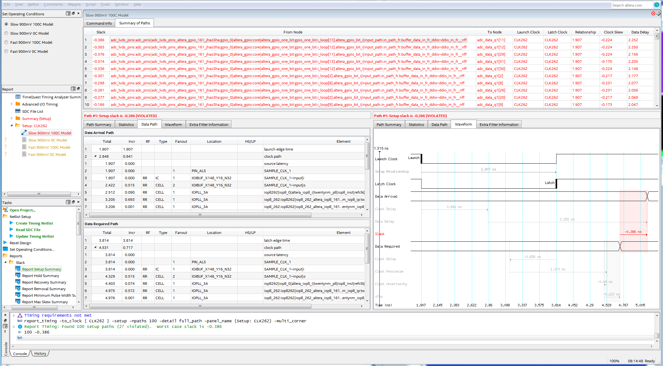
I have a setup violation at the register after the input register. The input register is constrained as described in AN433. set_input_delay -add_delay -clock virt_adc_clk -min -0.6 [get...

KhaiChein_Y_Intel Regular Contributor
7 years agoRegular ContributorHi,
I checked in the Timing Analyzer. The register is located within the I/O. According to the user guide https://www.intel.com/content/dam/www/programmable/us/en/pdfs/literature/ug/ug_altera_gpio.pdf, you may set the delay elements manually in the Intel Quartus Prime settings file (.qsf).
Input Delay Element
set_intance_assignment –to <PIN> -name INPUT_DELAY_CHAIN <0..63>
Output Delay Element set_intance_assignment –to <PIN> -name OUTPUT_DELAY_CHAIN <0..15>
Output Enable Delay Element
set_intance_assignment –to <PIN> -name OE_DELAY_CHAIN <0..15>
You may try to set the max and min value and see if it helps the timing. If no, this is the maximum frequency you can achieve with the I/O standard you have set, 1.8V
Thanks.