Forum Discussion

Altera_Forum's avatar
Altera_Forum
Icon for Honored Contributor rankHonored Contributor
12 years ago

This circuit to Verilog model.. Is it possible?

My background is on pure Digital design on verilog coding. My friend ask me if it is possible

to model the bellow circuit into verilog and use the verilog codes to DE0-NANO FPGA board.

If it is possible how can you connect an analog signal to DE0-NANO board. My Idea is

the function of "voltage-follower", "bias" and "Gain" can be modeled in verilog once

the analog signal is turn to digital signal. I believe DE0-NANO has a ADC function which

can do the job.

*p.s. please see fig below

https://www.alteraforum.com/forum/attachment.php?attachmentid=7056

I would appreciate any guidance about this matter.

Regards,

jayson
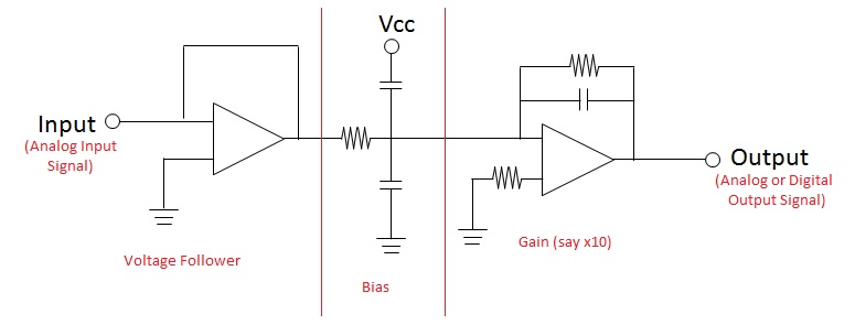
3 Replies

  • Altera_Forum's avatar
    Altera_Forum
    Icon for Honored Contributor rankHonored Contributor

    Apart from some errors in the analog schematic, Verilog doesn't model analog circuits. You can't simply "turn the analog signal to a digital signal". You need to design a time-discrete equivalent (by using z-transformation) of the time-continuous circuit and represent it in digital logic.

    de0-nano has an ADC, but no DAC to convert the digital signal to analog again.
  • Altera_Forum's avatar
    Altera_Forum
    Icon for Honored Contributor rankHonored Contributor

    Thank you FvM for the reply.

    So it is not possible to just model the function of the circuit into a verilog digital block?

    We would just like to make a project that takes in analog signal (do an ADConversion) create bias for it and apply some gain.

    It is ok for us if the output in the DE0-NANO is in digital equivalent signal.

    I hope you can still help us.

    Regards,

    jayson
  • Altera_Forum's avatar
    Altera_Forum
    Icon for Honored Contributor rankHonored Contributor

    You should specifiy the signal processing exactly. The schematic doesn't seem to implement a "bias". I guess you meaned to sketch a high-pass rather than the shown low-pass.

    But either if it's a high- or low-pass, it implements a time constant that would be approximated by a z-domain difference equation, the same for the output low-pass. If you don't actually mean it, correct the schematic.