Forum Discussion

 Occasional Contributor
CYCLONE IVE ODDR delay mismatch
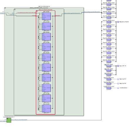
 5 months ago
The routing delay difference due to different type of pin assigned.
The bit fpga_dac_CHA[3] using this type of pin:
While other bits using these type of pin:
Different pin type will have different internal routing delay and this is fix one which cannot be changed.
So if change bit fpga_dac_CHA[3] and fpga_dac_CHB[3] pins to for example PIN_115 and PIN_120. The timing will be similar for all bits:
 Occasional Contributor
Thank you ShengN and thank you cblixt1.
So my suspicion about the Vref pins is confirmed.
cblixt1: regarding the false path issue, I have some doubts:
The oddr register that I am using is capable of launching the data on both the rising and falling edges of the clock. The dac_clk, instead, latches only on the rising edge. The values on the D inputs of the oddr register are updated (by other logic not currently present) only on the rising edge.
I can't understand which false paths are correct to insert in this situation..

 New Contributor
I added this
set_false_path \
  -fall_from [get_clocks {PLL1|altpll_component|auto_generated|pll1|clk[0]}] \
  -rise_to   [get_clocks {clk_dac_a}]
into your sdc file, and that seemed to do the trick. The Timing Analyzer now says


