Forum Discussion

Altera_Forum's avatar
Altera_Forum
Icon for Honored Contributor rankHonored Contributor
12 years ago

Accessing SDRAM memory on Terasic DE0-Nano board.

I want to use SDRAM memory located on DE0-Nano board using Verilog (without using Nios).

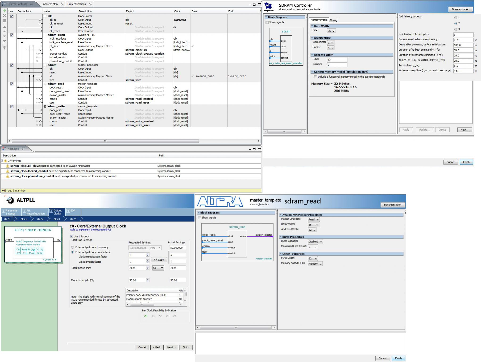
I use http://www.altera.com/support/examples/nios2/exm-avalon-mm.html

System placed in the QSYS:

https://www.alteraforum.com/forum/attachment.php?attachmentid=8357

sdram_write not currently used.

Code:

//=======================================================
module SRAM(
CLOCK_50, LED,
DRAM_ADDR, DRAM_BA, DRAM_CAS_N, DRAM_CKE, DRAM_CLK, DRAM_CS_N, DRAM_DQ, DRAM_DQM, DRAM_RAS_N, DRAM_WE_N //Memory pin
);
//////////// CLOCK //////////
input                           CLOCK_50;
//////////// LED //////////
output                     LED;
//reg                         LED;
//////////// SDRAM //////////
output                    DRAM_ADDR;
output                     DRAM_BA;
output                          DRAM_CAS_N;
output                          DRAM_CKE;
output                          DRAM_CLK;
output                          DRAM_CS_N;
inout                     DRAM_DQ;
output                     DRAM_DQM;
output                          DRAM_RAS_N;
output                          DRAM_WE_N;
//////////// AVALON MASTER TEMPLATE //////////
wire        qsys_sdram_read_control_fixed_location;
wire         qsys_sdram_read_control_read_base;
wire         qsys_sdram_read_control_read_length;
wire        qsys_sdram_read_control_go;
reg        reg_qsys_sdram_read_control_fixed_location;
reg         reg_qsys_sdram_read_control_read_base;
reg         reg_qsys_sdram_read_control_read_length;
reg        reg_qsys_sdram_read_control_go;
wire        qsys_sdram_read_control_done;
wire        qsys_sdram_read_control_early_done;
wire        qsys_sdram_read_user_read_buffer;
reg        reg_qsys_sdram_read_user_read_buffer;
wire         qsys_sdram_read_user_buffer_output_data;
wire        qsys_sdram_read_user_data_available;
reg gooff=0;
reg rboff=0;
reg init=1;
qsys u0(
        .clk_clk(CLOCK_50),                                //clk.clk
        .reset_reset_n(1'b1),                            //reset.reset_n
        
        .sdram_clock_c0_clk(DRAM_CLK),                //sdram_clock_c0.clk
        .sdram_clock_areset_conduit_export(1'b0),    //sdram_clock_areset_conduit.export
        
        .sdram_wire_addr(DRAM_ADDR),                    //sdram_wire.addr
        .sdram_wire_ba(DRAM_BA),                        //           .ba
        .sdram_wire_cas_n(DRAM_CAS_N),                //           .cas_n
        .sdram_wire_cke(DRAM_CKE),                        //           .cke
        .sdram_wire_cs_n(DRAM_CS_N),                    //           .cs_n
        .sdram_wire_dq(DRAM_DQ),                        //           .dq
        .sdram_wire_dqm(DRAM_DQM),                        //           .dqm
        .sdram_wire_ras_n(DRAM_RAS_N),                //           .ras_n
        .sdram_wire_we_n(DRAM_WE_N),                    //           .we_n
        
        .sdram_read_control_fixed_location(qsys_sdram_read_control_fixed_location),
        .sdram_read_control_read_base(qsys_sdram_read_control_read_base),
        .sdram_read_control_read_length(qsys_sdram_read_control_read_length),
        .sdram_read_control_go(qsys_sdram_read_control_go),
        .sdram_read_control_done(qsys_sdram_read_control_done),
        .sdram_read_control_early_done(qsys_sdram_read_control_early_done),
        .sdram_read_user_read_buffer(qsys_sdram_read_user_read_buffer),
        .sdram_read_user_buffer_output_data(qsys_sdram_read_user_buffer_output_data),
        .sdram_read_user_data_available(qsys_sdram_read_user_data_available)
);
assign qsys_sdram_read_control_fixed_location = reg_qsys_sdram_read_control_fixed_location;
assign qsys_sdram_read_control_read_base  = reg_qsys_sdram_read_control_read_base ;
assign qsys_sdram_read_control_read_length  = reg_qsys_sdram_read_control_read_length ;
assign qsys_sdram_read_control_go = reg_qsys_sdram_read_control_go;
assign qsys_sdram_read_user_read_buffer = reg_qsys_sdram_read_user_read_buffer;
always @(posedge CLOCK_50)
begin
    if (gooff)
    begin
        gooff <= 0;
        reg_qsys_sdram_read_control_go <= 0;
    end
    
    if (init)
    begin
        reg_qsys_sdram_read_control_fixed_location <= 0;
        reg_qsys_sdram_read_control_read_base <= 0;
        reg_qsys_sdram_read_control_read_length <= 8;
        reg_qsys_sdram_read_control_go <= 1;
        gooff <= 1;
        init <= 0;
    end
    
end
assign LED  = qsys_sdram_read_user_buffer_output_data ;
endmodule

Memory is not written so it should read garbage and display on the LEDs, but the LEDs do not light.

16 Replies

  • Altera_Forum's avatar
    Altera_Forum
    Icon for Honored Contributor rankHonored Contributor

    Hello,

    I want to write SDRAM through my custom hardware IP. I am using the Master Templates for this. I am writing using custom hardware and reading using NIOS, but my bios doesn't read the correct value.

    Below is my code for writing into SDRAM.

    I want to write on the click of a button (coe_switch[3]). I have one more doubt, "myBuffer_control_write_write_base" should be the base address for SDRAM or offset or base+offest.

    reg searchForSync;

    always @(posedge csi_clk or negedge rsi_rst) begin

    if(!rsi_rst) begin

    click <= 0;

    searchForSync <= 0;

    end else begin

    if(coe_switch[3] == 0) begin

    searchForSync <= 1;

    myBuffer_control_write_fixed_location <= 0;

    myBuffer_control_write_write_base <= 32'h00000000;

    myBuffer_control_write_write_length <= 8;

    myBuffer_control_write_go <= 1;

    myBuffer_user_write_buffer_input_data <= 1;

    myBuffer_user_write_write_buffer <= 1;

    end

    if(searchForSync == 1) begin

    myBuffer_user_write_buffer_input_data <= 1;

    myBuffer_user_write_write_buffer <= 1;

    myBuffer_control_write_go <= 0;

    if(asi_stin_sop_reg[319] == 1) begin

    end

    end

    end

    end

    Please let me know if I am doing something wrong.

    Please suggest.
  • Altera_Forum's avatar
    Altera_Forum
    Icon for Honored Contributor rankHonored Contributor

    --- Quote Start ---

    Problem fixed. Need to wait two clock tacts before reading.

    --- Quote End ---

    Hello,

    Did you tried writing into SDRAM. I am trying but couldn't get the result.

    Please check my post on the same thread.

    Thanks
  • Altera_Forum's avatar
    Altera_Forum
    Icon for Honored Contributor rankHonored Contributor

    Post your problem in a new thread. Then more people will see it, not just those subscribed to this thread :).

    Tip: please post more detail then you already have. The information you've posted isn't really enough. E.g. what does the code for your 'custom hardware IP' look like? Please wrap any code posted with code tags...

    Regards,

    Alex
  • Altera_Forum's avatar
    Altera_Forum
    Icon for Honored Contributor rankHonored Contributor

    Dear Mikel7,

    I would use a on Deo Nano board the SDRAM without using the Nios || processor, could you share your working code for SDRAM?

    Thanks in advances,

    Alexgiul
  • Altera_Forum's avatar
    Altera_Forum
    Icon for Honored Contributor rankHonored Contributor

    I'am not used this board for long time, but this should work:

    //=======================================================
    module SRAM(
    CLOCK_50, LED, KEY,
    DRAM_ADDR, DRAM_BA, DRAM_CAS_N, DRAM_CKE, DRAM_CLK, DRAM_CS_N, DRAM_DQ, DRAM_DQM, DRAM_RAS_N, DRAM_WE_N //Memory pin
    );
    //////////// CLOCK //////////
    input 		          		CLOCK_50;
    //////////// LED //////////
    output		     		LED;
    reg			     		LED;
    //////////// KEY //////////
    input		KEY;
    //////////// SDRAM //////////
    output		    		DRAM_ADDR;
    output		     		DRAM_BA;
    output		          		DRAM_CAS_N;
    output		          		DRAM_CKE;
    output		          		DRAM_CLK;
    output		          		DRAM_CS_N;
    inout 		    		DRAM_DQ;
    output		     		DRAM_DQM;
    output		          		DRAM_RAS_N;
    output		          		DRAM_WE_N;
    //////////// AVALON CONNECTOR //////////
    wire		qsys_sdram_read_control_fixed_location;
    wire		 qsys_sdram_read_control_read_base;
    wire		 qsys_sdram_read_control_read_length;
    wire		qsys_sdram_read_control_go;
    reg		reg_qsys_sdram_read_control_fixed_location;
    reg		 reg_qsys_sdram_read_control_read_base;
    reg		 reg_qsys_sdram_read_control_read_length;
    reg		reg_qsys_sdram_read_control_go;
    wire		qsys_sdram_read_control_done;
    wire		qsys_sdram_read_control_early_done;
    wire		qsys_sdram_read_user_read_buffer;
    reg		reg_qsys_sdram_read_user_read_buffer;
    wire		 qsys_sdram_read_user_buffer_output_data;
    wire		qsys_sdram_read_user_data_available;
    reg gooff=0;
    integer start=3;
    qsys u0(
    		.clk_clk(CLOCK_50),								//clk.clk
    		.reset_reset_n(1'b1),							//reset.reset_n
    		
    		.sdram_clock_c0_clk(DRAM_CLK),				//sdram_clock_c0.clk
    		.sdram_clock_areset_conduit_export(1'b0),	//sdram_clock_areset_conduit.export
    		
    		.sdram_wire_addr(DRAM_ADDR),					//sdram_wire.addr
    		.sdram_wire_ba(DRAM_BA),						//           .ba
    		.sdram_wire_cas_n(DRAM_CAS_N),				//           .cas_n
    		.sdram_wire_cke(DRAM_CKE),						//           .cke
    		.sdram_wire_cs_n(DRAM_CS_N),					//           .cs_n
    		.sdram_wire_dq(DRAM_DQ),						//           .dq
    		.sdram_wire_dqm(DRAM_DQM),						//           .dqm
    		.sdram_wire_ras_n(DRAM_RAS_N),				//           .ras_n
    		.sdram_wire_we_n(DRAM_WE_N),					//           .we_n
    		
    		.sdram_read_control_fixed_location(qsys_sdram_read_control_fixed_location),
    		.sdram_read_control_read_base(qsys_sdram_read_control_read_base),
    		.sdram_read_control_read_length(qsys_sdram_read_control_read_length),
    		.sdram_read_control_go(qsys_sdram_read_control_go),
    		.sdram_read_control_done(qsys_sdram_read_control_done),
    		.sdram_read_control_early_done(qsys_sdram_read_control_early_done),
    		.sdram_read_user_read_buffer(qsys_sdram_read_user_read_buffer),
    		.sdram_read_user_buffer_output_data(qsys_sdram_read_user_buffer_output_data),
    		.sdram_read_user_data_available(qsys_sdram_read_user_data_available)
    );
    assign qsys_sdram_read_control_fixed_location = reg_qsys_sdram_read_control_fixed_location;
    assign qsys_sdram_read_control_read_base  = reg_qsys_sdram_read_control_read_base ;
    assign qsys_sdram_read_control_read_length  = reg_qsys_sdram_read_control_read_length ;
    assign qsys_sdram_read_control_go = reg_qsys_sdram_read_control_go;
    assign qsys_sdram_read_user_read_buffer = reg_qsys_sdram_read_user_read_buffer;
    always @(posedge CLOCK_50)
    begin
    	if (start==1)
    	begin
    		reg_qsys_sdram_read_control_fixed_location <= 0;
    		reg_qsys_sdram_read_control_read_base <= 0;
    		reg_qsys_sdram_read_control_read_length <= 2;
    		reg_qsys_sdram_read_control_go <= 1;
    		gooff <= 1;
    	end
    	if (gooff)
    	begin
    		gooff <= 0;
    		reg_qsys_sdram_read_control_go <= 0;
    	end
    	if (start) start = start - 1;
    	LED  <= qsys_sdram_read_user_buffer_output_data ;
    end
    endmodule