Forum Discussion

Altera_Forum Honored Contributor
10 years agoHonored ContributorAbout VGA Output
Hello,
I am working for the first time with FPGA (cyclone v soc) and i am trying to get a output from VGA Port on the monitor. I have set the resolution for 1024x768 and PLL input frequency as 50MHz and output frequency as 65MHz as required for the resolution.But as soon as i program the board the monitor is going to sleep mode. I am attaching the code which i used for this. Can you please tell me what may be the problem. When I checked in RTL Simulation PLL is not generating any clock output. Thank you in advance. Code: ----Main code LIBRARY IEEE; USE IEEE.STD_LOGIC_1164.ALL; USE IEEE.NUMERIC_STD.ALL; ENTITY VGA IS PORT( CLOCK_24: IN STD_LOGIC; SYS_rst : IN STD_LOGIC; VGA_HS, VGA_VS: OUT STD_LOGIC; VGA_R, VGA_G, VGA_B: OUT STD_LOGIC_VECTOR(7 DOWNTO 0); VGA_CLK_65MHZ : OUT STD_LOGIC ); END VGA; ARCHITECTURE MAIN OF VGA IS SIGNAL VGACLK, RESET, lock : STD_LOGIC :='0'; signal SIGNAL_135MHZ : STD_LOGIC:= '0'; COMPONENT SYNC IS PORT ( CLK : IN STD_LOGIC; HSYNC, VSYNC : out std_logic; R, G, B : OUT STD_LOGIC_VECTOR(7 DOWNTO 0) ); END COMPONENT; component unsaved is -- PLL Component port ( pll_0_locked_export : out std_logic; -- pll_0_locked.export pll_0_outclk0_clk : out std_logic; -- clk pll_0_refclk_clk : in std_logic := '0'; -- clk pll_0_reset_reset : in std_logic := '0' -- reset ); end component unsaved; BEGIN inst_pll : UNSAVED port map ( pll_0_refclk_clk => clock_24, pll_0_reset_reset => SYS_rst, pll_0_outclk0_clk => VGACLK, ---CLOCK 65 MHZ --outclk_1 => SIGNAL_135MHZ, --- CLOCK 135 MHZ pll_0_locked_export => lock ); INST_SYNC : SYNC PORT MAP ( CLK => VGACLK, HSYNC => VGA_HS, VSYNC => VGA_VS, R => VGA_R, G => VGA_G, B => VGA_B ); VGA_CLK_65MHZ <= VGACLK; END MAIN; ---Sub Program LIBRARY IEEE; USE IEEE.STD_LOGIC_1164.ALL; USE IEEE.NUMERIC_STD.ALL; ENTITY SYNC IS PORT( CLK : IN STD_LOGIC; HSYNC, VSYNC : out std_logic; R, G, B : OUT STD_LOGIC_VECTOR(7 DOWNTO 0) ); END SYNC; ARCHITECTURE MAIN OF SYNC IS SIGNAL HPOS: INTEGER RANGE 0 TO 1344:=0; SIGNAL VPOS: INTEGER RANGE 0 TO 806:=0; BEGIN PROCESS(CLK,HPOS,VPOS) BEGIN IF(CLK' EVENT AND CLK='1') THEN IF (HPOS = 832 OR VPOS = 422) THEN R <= (OTHERS => '1'); G <= (OTHERS => '1'); B <= (OTHERS => '1'); ELSE R <= (OTHERS => '0'); G <= (OTHERS => '0'); B <= (OTHERS => '0'); END IF; IF(HPOS<1344) THEN HPOS <= HPOS+1; ELSE HPOS <=0; END IF; IF (VPOS<806)THEN VPOS <= VPOS+1; ELSE VPOS <=0; END IF; END IF; IF (HPOS > 24 AND HPOS < 160)THEN HSYNC <= '0'; ELSE HSYNC <= '1'; END IF; IF (VPOS > 3 AND VPOS < 9) THEN VSYNC <= '0'; ELSE VSYNC <= '1'; END IF; IF ((HPOS> 0 AND HPOS< 320) OR (VPOS>0 AND VPOS< 38)) THEN R <= (OTHERS => '0'); G <= (OTHERS => '0'); B <= (OTHERS => '0'); END IF; END PROCESS; END MAIN;28 Replies
 Altera_Forum
- Altera_Forum
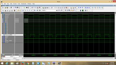
I'm sorry but the waveform is not visible. Is the 65MHz clock output fine now?
- Altera_Forum
- Altera_Forum
According to your logic, the RGB data remains zero at all times, except at this condition
IF (HPOS = 832 OR VPOS = 422) THEN R <= (OTHERS => '1'); G <= (OTHERS => '1'); B <= (OTHERS => '1'); So what are you expecting on the display? And is there any decoder on the output path to be configured? - Altera_Forum
hi,
I want to draw one vertical and one horizontal line at the middle of the screen. decoder on the output path..?? no i guess - Altera_Forum
Then it looks fine. If its fine in simulation then it should be working on board
- Altera_Forum
may i ask you what do u mean by configuring the decoder on the output path....??
i dont know why monitor is going to power saving mode. Its Dell LCD monitor with maximum resolution of 1366x768. Should i try with old CRT monitor..? - Altera_Forum
pnayak15 -
What is driving the monitor? Is the FPGA output going to a DVI or HDMI transmitter? If so, what is driving the DE input to the transmitter? I can't see your simulation waveforms because your JPEGs are too small, but from your VHDL code it looks like the PLL is held in reset. Are you sure your clocking is ok? Can you probe your clock on the board to verify? - Altera_Forum
hii rsefton,
VGA clock output is driving the monitor. Is the PLL Held in RESET.?? I am not sure whether the output is proper but im getting continuous vga clock output pulses. I can you mail you the simulation waveform if it is fine. Please drop a empty mail at [email protected] I really need to get it sorted soon Thank you - Altera_Forum
Hi pnayak15 -
It's not possible to drive a monitor directly with 27 2.5V signals (VGA_CLK, VGA_VS, VGA_HS, VGA_R[7:0], VGA_G[7:0], VGA_B[7:0]). There must be an encoder/transmitter IC between the FPGA and the monitor (I assume DVI or HDMI). These transmitter ICs typically have a DE (data enable) input that must be driven. If you don't drive that signal then you won't get a valid signal to the monitor. What is between the FPGA and monitor? Include everything, including (transmitter, connector, cable, etc). And what model of monitor are you driving?