Forum Discussion

Altera_Forum Honored Contributor
9 years agoHonored Contributorpin assignment problem
Hi,
I am new to quartus ii. I have created a bdf file instead of verilog/vhdl . i am taking input through terasic data conversion card and through sma cable i am giving a sine wave but i am not able to see the input through signal tap analyzer . when i see the pin planner there is no location , bank and pin assigned to inputs and outputs . i have imported the pin assignments. what can i do so the output and input will be assigned. Help will be highly appreciated. Thanks in Advance16 Replies
 Altera_Forum--- Quote Start --- There will be at least an automatically selected fitter location shown for each port signal after compilation if you didn't assign a location. Did you select a FPGA type in device assignments? How? --- Quote End --- Hi, Yeah there is automatic selected fitter but the i cant find the correct input in signal tap. i have attached a screenshot of pin planner.
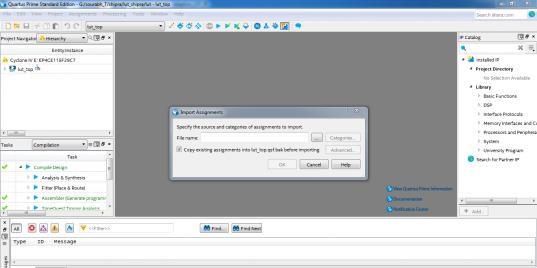
- Altera_Forum--- Quote Start --- Hi shipra7993, I have never heard importing pin assignments method in Quartus II/Prime software. As far I have done which is known to be working is either, assigning the pin manually one-by-one or copy and paste a list of the pins into the Pin Assignment. I would recommend that you cross check the schematics for the correct pins to be assign in the Pin Assignment especially the clock pins which is a must in order to run the Signal Tap. Regards, nyusof (This message was posted on behalf of Intel Corporation) --- Quote End --- Hi Nyusof, Thanks! I have attached the screenshot of the import assignments, that is what i did for pin assignments but i am not getting the desired input and when i manually assign pin it doesn't accepts. Regards, Shipra
- Altera_Forum--- Quote Start --- Hi, I am new to quartus ii. I have created a bdf file instead of verilog/vhdl . i am taking input through terasic data conversion card and through sma cable i am giving a sine wave but i am not able to see the input through signal tap analyzer . when i see the pin planner there is no location , bank and pin assigned to inputs and outputs . i have imported the pin assignments. what can i do so the output and input will be assigned. Help will be highly appreciated. Thanks in Advance --- Quote End --- Hi shipra7993, I have never heard importing pin assignments method in Quartus II/Prime software. As far I have done which is known to be working is either, assigning the pin manually one-by-one or copy and paste a list of the pins into the Pin Assignment. I would recommend that you cross check the schematics for the correct pins to be assign in the Pin Assignment especially the clock pins which is a must in order to run the Signal Tap. Regards, nyusof (This message was posted on behalf of Intel Corporation)
- Altera_Forum--- Quote Start --- when i see the pin planner there is no location , bank and pin assigned to inputs and outputs --- Quote End --- There will be at least an automatically selected fitter location shown for each port signal after compilation if you didn't assign a location. Did you select a FPGA type in device assignments? --- Quote Start --- I have imported the pin assignments --- Quote End --- How?