Altera_Forum Honored Contributor
Honored ContributorHonored ContributorHi,
I'm currently building a low cost FPGA board for my school project. Referencing to DE0 schematic diagram for USB Blaster circuit: 1) What is the value of L1 & L2? and what does BEAD means? 2) If I'm using CYCLONE EP1C3T100 chip, where do I connect the nRESET to? 3) What is CPLD ISP? Is there any part no. or model no. for it? I have attached the schematic dwg for reference. Frankly, I'm quite new to FPGA. Pls helpHonored ContributorHi:
1: L1 and L2, you need to reference the Build of Materials (BOM) for the DE0 board. It should give you a part number. Those are Ferrite beads. Typically they are surface mount devices in a 0603 or 0402 package on these boards. 2: Apparently nReset is not used in their design. They tied it off, but you could do with it what you want. I like a push button if space is not an issue. 3: The CPLD_ISP is a standard 10 pin header, used to connect a USB-blaster to the board to initially program the CPLD. PeteHonored ContributorDo you have a *.pof file for the USB Blaster CPLD?
Honored ContributorTake heed of FvM's comment. Are you trying to make a board with the USB blaster circuit on it? This includes an Altera CPLD programmed with code. Does your school have access to that code?
Assuming they don't (I think that likely), I recommend your school buys Altera's off the shelf USB-Blaster cable to program your Cyclone FPGA. http://www.altera.co.uk/literature/ug/ug_usb_blstr.pdfHonored ContributorSo I need a code to program the CPLD to configure the USB blaster circuit.
Therefore there is no point of me making USB blaster circuit on the board as in the end I still need to buy the USB blaster download cable for the CPLD programming. Thank you very much to everyone for all the advices.Honored ContributorYes.
Terasic makes a cheap USB-blaster clone, for $50.00. It works well. http://www.terasic.com.tw/cgi-bin/page/archive.pl?language=english&categoryno=74 PeteHonored ContributorHi,
I have discuss with my school and they allow me to buy the USB blaster cable. Now I have a simpler design for this project. Anyway, can I design a simple FPGA board with just basic i/o without any external memory? My target is just to download simple logic block diagram onto it test using the i/o. I have assigned some pins to the i/o. Can someone help to verify if the assignment is correct? Thank you.Honored ContributorYes, you can design a board without any external memory. However, when powered up your board will have no ability to boot the FPGA itself. You will need to use the USB-Blaster every time you switch the board on. For a school project, I'd suggest that is acceptable.
A quick look round the diagram you posted doesn't highlight anything untoward. Minor comment: you have a (very slow) clock feeding two clock pins. You only really need drive one clock pin and you'll be able to use it through the device. Tie the second clock input pin to GND or drive it with a different clock frequency to control some other exciting logic. Do you mean 50Hz? That is a very slow clock for and FPGA :). They typically run at, perhaps, 50MHz...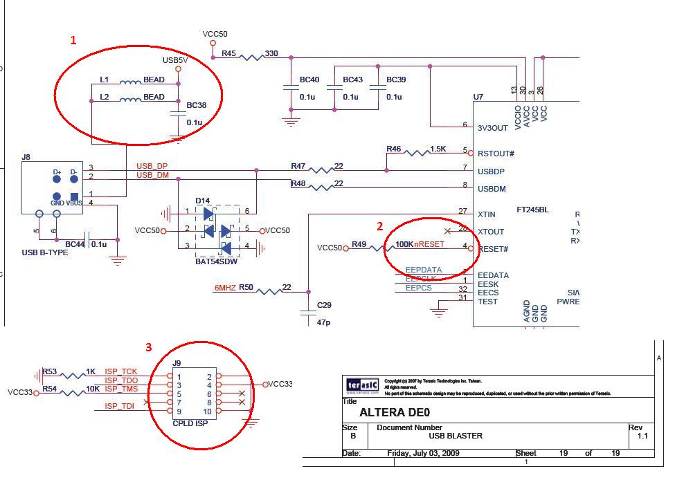