Forum Discussion

Altera_Forum Honored Contributor
12 years agoHonored Contributorinductor value in usb blaster and what is CPLD ISP part no
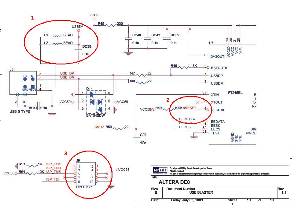
Hi, I'm currently building a low cost FPGA board for my school project. Referencing to DE0 schematic diagram for USB Blaster circuit: 1) What is the value of L1 & L2? and what does BEAD me...

Altera_ForumHonored Contributor
12 years agoHonored ContributorYes, you can design a board without any external memory. However, when powered up your board will have no ability to boot the FPGA itself. You will need to use the USB-Blaster every time you switch the board on. For a school project, I'd suggest that is acceptable.
A quick look round the diagram you posted doesn't highlight anything untoward. Minor comment: you have a (very slow) clock feeding two clock pins. You only really need drive one clock pin and you'll be able to use it through the device. Tie the second clock input pin to GND or drive it with a different clock frequency to control some other exciting logic. Do you mean 50Hz? That is a very slow clock for and FPGA :). They typically run at, perhaps, 50MHz...