Forum Discussion

 New Contributor
How well FPGA adjust delays based on .sdc
- 2 years ago
Perhaps sstrell could help to clarify more on your first question.
Anyhow, we uses one of the two methods in deriving the input and output constraints for the SS.
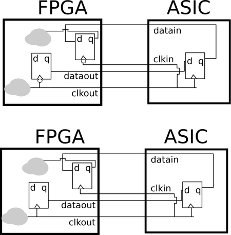
From what I see in the diagram, you may consider using the system-centric method.By specifying the appropriate clock waveform using the -waveform option, you can effectively align the clock edges to accommodate the data transfer requirements. Whether you choose center alignment or edge alignment depends on your specific design needs.
You may checkout the "Clock and Data Relationship" section in AN433 and below screenshot.
Regards,
Richard Tan
 New Contributor
Hi Richard and sstrell,
Thank you for your answers. I was just trying to figure out the 2) answer. Why the first way is incorrect? It's incorrect in the sense that the .sdc constraints are wrong or the general approach with rising-to-falling transition is wrong? In the end we have 2 source synchronous interfaces. I know I forgot to add the declaration of virtual clock clkin.
Is 1) actually an answer to the above mentioned question? Do I understand correctly, the proposed center alignment information added in the clock declaration (-waveform ) should eliminate the clock_fall attribute. In the end the information about falling edge aligned data is synonymous to center rising edge aligned data.

 Super Contributor
Perhaps sstrell could help to clarify more on your first question.
Anyhow, we uses one of the two methods in deriving the input and output constraints for the SS.
From what I see in the diagram, you may consider using the system-centric method.
By specifying the appropriate clock waveform using the -waveform option, you can effectively align the clock edges to accommodate the data transfer requirements. Whether you choose center alignment or edge alignment depends on your specific design needs.
You may checkout the "Clock and Data Relationship" section in AN433 and below screenshot.
Regards,
Richard Tan


