Forum Discussion

 New Contributor
How well FPGA adjust delays based on .sdc
- 2 years ago
Perhaps sstrell could help to clarify more on your first question.
Anyhow, we uses one of the two methods in deriving the input and output constraints for the SS.
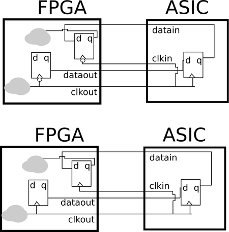
From what I see in the diagram, you may consider using the system-centric method.By specifying the appropriate clock waveform using the -waveform option, you can effectively align the clock edges to accommodate the data transfer requirements. Whether you choose center alignment or edge alignment depends on your specific design needs.
You may checkout the "Clock and Data Relationship" section in AN433 and below screenshot.
Regards,
Richard Tan


 Super Contributor
To paraphrase, "There's an app [note] for that" as well as a training:
https://learning.intel.com/developer/learn/courses/168/constraining-source-synchronous-interfaces
Answering your questions:
1) Clock latency constraints and generated clock for input clock are not needed. Just use create_clock for the virtual clock driven by the external device (launch edge) and for the clock arriving at the FPGA (latch edge), either center aligned or edge aligned using the -waveform option of create_clock. set_input_delay will refer to the virtual clock to select the launch edge clock and calculated max/min values will be based off info from external device (tco, setup/hold requirements, or skew). If tco is used, trace delay differences can be included in the calculation.
2) Method 1 is not really correct for constraining an SS interface.
3) Better idea would be to use the DDIO registers. Even if this is single data rate, you can tie the low data input to the high data input. The DDIO registers provide matching delay for the clock and data for both inputs and outputs.
4) Not relevant if DDIO registers are used.
5) Timing constraints guide the Fitter to meet the timing requirements you specify. Fine tuning may be possible in hardware for particular devices as you note, but it's not normally required. The constraints handle everything.


