JFrye7 New Contributor
New ContributorNew Contributor Regular Contributor
Hi,
Can you check if you have set the correct base addresses of the slaves in your design that is connected to the HPS AXI master bridge?:
https://www.intel.com/content/www/us/en/programmable/hps/cyclone-v/hps.html
New ContributorHPS AXI has already been verified. I have software that can read and write the registers in my address map. I can write the DMA registers with my Linux user space application and read them back.
That offset in my software is 0xFF200000. I use /dev/mem to open and read the HPS AXI register space.
As far as FPGA2SDRAM bridge goes, I do have an update. By performing these two writes in U-Boot, I can at least get the address address ready signals for ports 0 and 1 (read and write ports for AXI) to assert.
# fpga-sdram bridge
mw FFC25080 00000311
mw FFC2505C 00000004
After the interface appears to accept the read address requests coming from the DMA master interface, it never asserts the signal on the port that corresponds to AXI RVALID and the kernel freezes, then the thing reboots.
Not sure what this might be. My guess is one of two things
1. Interface registers are still not configured correctly
2. Platform Design HPS block has wrong DDR timing configurations.
If the HPS is set up with the wrong DDR timing parameters, would the ARM still be able to perform load/store instructions (because it obviously since it is successfully able to run u-boot and the OS)?
New ContributorAlso worth noting my board is DE1-SoC, so it might have different timing parameters than your board for the DDR.
Regular ContributorHi,
Is this your own design image? It may boot up with wrong DDR timings but it is never recommended, you may need to follow the timing specs of the DDR that you are using and set it correctly in Platform Designer, have you try running with the exact timing specs yet?
New ContributorI have gotten the FPGA2SDRAM interface to work with updated version of both embedded_command_shell and u-boot-socfpga.
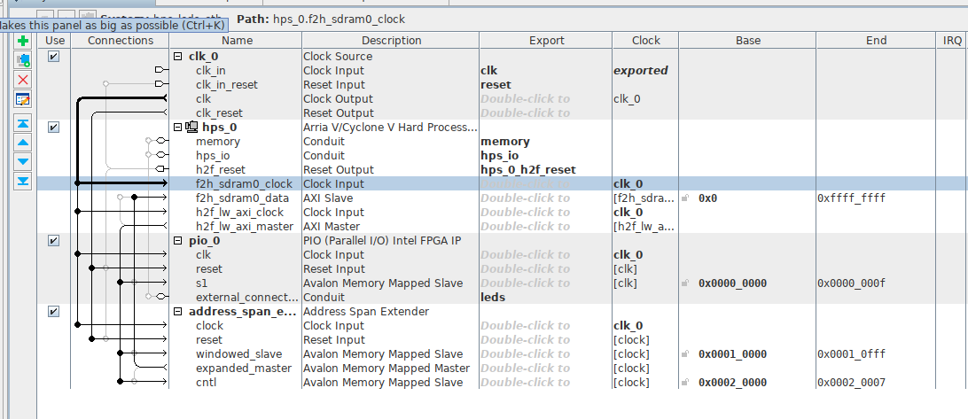
My next question (maybe I need to open another ticket about this) is about addressing. I have a similar design with an address space extender IP with which I attempt to write to the SDRAM interface through the fabric.
Essentially as I understand it, by writing to the IP window register, I can get access to certain windows in the master address space "expanded master". I can then initiate transactions to the address span extender slave address space windowed_slave to trigger corresponding transactions on the extender_master interface based on what is programmed into the offset register.
In u-boot I attempt to write to addresses in the SDRAM using an address space extender. This address is within the first GB of the SDRAM. I then try to read back the address via the u-boot md command, but the data displayed is inconsistent with what was written through the fabric via address span extender. When I read back using address span extender, it matches what was written.
How addresses look different from perspective of FPGA2SDRAM interface vs from the HPS?