Altera_Forum Honored Contributor
11 years agoHonored ContributorConstraining Complex Design in SDC
Hi,
I've been working on a fairly complex design which has several external devices (two ADCs, a DAC, and four voltage pulsers) which each have have clock and data lines that need constraining to check that they will meet the required setup/hold specs. What gets a bit complex is that each IC will have its clock sourced from the FPGA to avoid the need for external LVDS clock buffers, but each clock within a group must remain as closely aligned as possible (no more than around 200ps out - ballpark figure), so for example the four pulser clocks must be aligned to each other, the two ADC clocks must be aligned. With the ADCs the clock that is fed out is a sample clock which goes in to the ADC and then is returned shifted by anywhere between 10.3ns and 12ns internally after which it comes out as an LVDS frame clock. This frame clock feeds back into the FPGA to deserialise LVDS two groups of 8 data channels which may also need constraining. The two frame clocks are shifted by 165 degrees during the deserialisation resulting in a parallel clock. Data is simply clocked back onto the original sample clock source to return it to the the sample clock domain so that the data from both ADCs is synchronised. I've attached a drawing of an overview of the system. I was wondering if someone could guide me through constraining this design as although I have read through several documents on timequest and source-synchronous signals, its not really sinking in and so I don't really know what I am doing (and the effect the commands are having) to put it bluntly. Any advice would be greatly appreciated.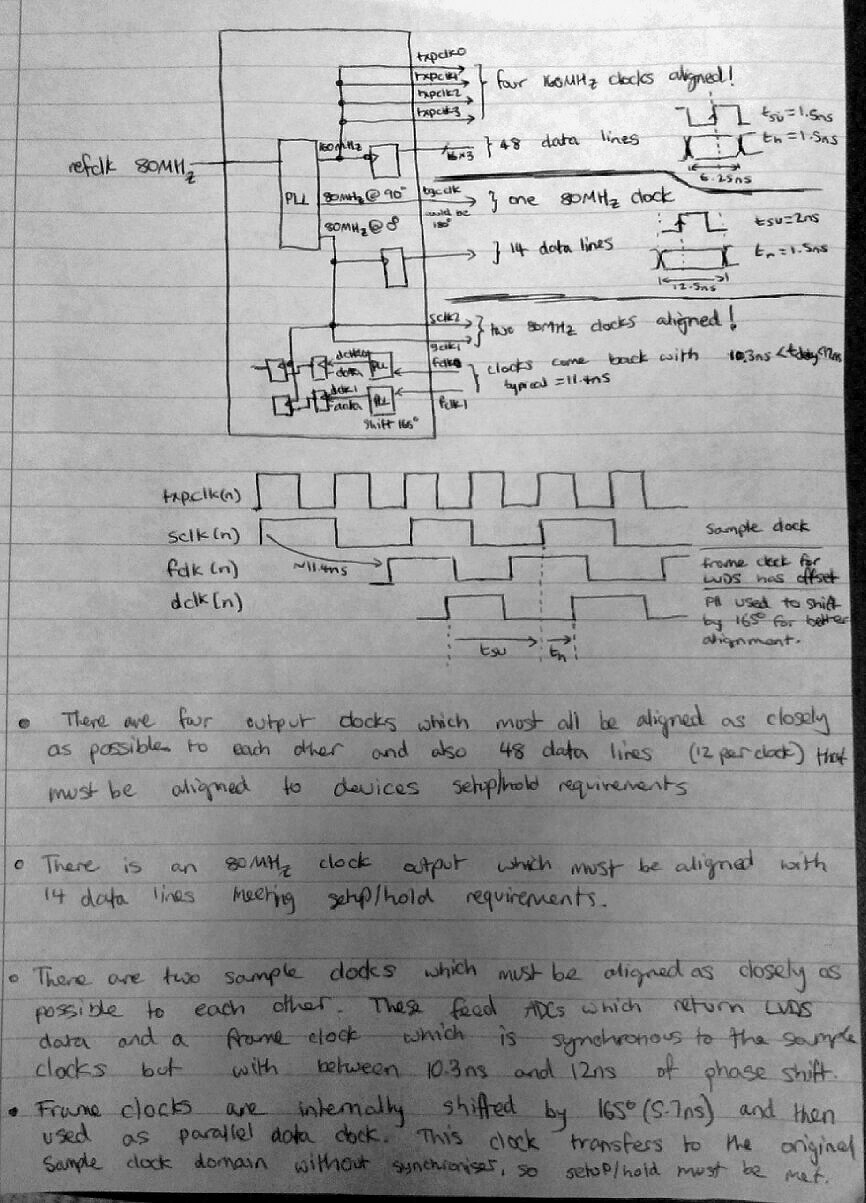