anaza3 New Contributor
New ContributorSharing SDRAM by two NIOS cores
 New Contributor
 Regular Contributor
HI,
DE0 board only contains 1 SDRAM memory device interface. Therefore, you can't create 2 SDRAM IP in QSYS.
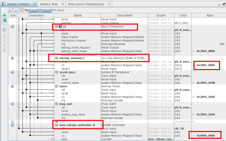
It would be easier to hook up everything under same QSYS interface rather than create sub-block design (core1, core2) to verify the design connection first. It's easier to manage to QSYS addressing as well.
For instance, using core1 sub-block design. I tried out following combination
You can read more about QSYS usage guideline in below link as well
Thanks.
Regards,
dlim