Forum Discussion

 New Contributor
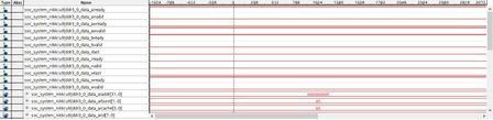
Hi , I am working with DE10-nano board to access external DDR3. FPGA-to-HPS SDRAM Interface- AXI3 is not working properly(axi_awready is always low)
 7 years ago
Dear NKRIS7,
I am sorry for the delay in response as I had to attend company's meeting yesterday. I truly apologize for the delay.
The waitrequest is a mechanism for throttling the source of traffic to the IO Slave port. If the waitrequest is asserted High (or in other word axi_awready is always low) , it means the IO slave port does not have enough resources to keep accepting the write burst. It requests some time to wait for data processing. So, may I know for how long is the waitrequest remain high ? Is it too long ?
By the way, I found a project on RocketBoards utilizing FPGA2SDRAM interfaces:
https://rocketboards.org/foswiki/Projects/CycleVSoCSDRAMPerformanceExampleDesign
Perhaps you can take a look on that. 😊
Also you may want to read through this KDB solution and check if any setting miss out :
https://www.intel.com/content/www/us/en/programmable/support/support-resources/knowledge-base/embedded/2016/how-and-when-can-i-enable-the-fpga2sdram-bridge-on-cyclone-v-soc.html
Thanks
Regards,
NAli1
 Frequent Contributor
Dear NKRIS7,
There are several example and demo related to AXI interface as per listed below. Hopefully this is helpful for you. If not,please don’t hesitate to ask for more details.😊
1) BFM Simulation Example: HPS AXI* Bridge Interface to FPGA Core:-
The Hard Processor System (HPS) in Intel SoC devices has a HPS-to-FPGA AXI* Bridge (h2f) interface for communicating with memories and peripherals in the FPGA core.
https://www.intel.com/content/www/us/en/programmable/support/support-resources/design-examples/design-software/qsys/exm-hps-axi-bfm.html
2) Demo AXI Memory Design Example:-
This design example demonstrates an AMBA* AXI*-3 slave interface on a simple Verilog custom memory component for Qsys systems. You can use this example as a basis for your own custom AXI slave interfaces.
https://www.intel.com/content/altera-www/global/en_us/index/support/support-resources/design-examples/design-software/qsys/exm-demo-axi3-memory.html
3) Designing with AXI for Altera SoC ARM Devices Workshop Lab - Instantiating Your AXI3 Component:-
https://fpgawiki.intel.com/wiki/Designing_with_AXI_for_Altera_SoC_ARM_Devices_Workshop_Lab_-_Instantiating_Your_AXI3_Component
Also, you may refer to this handbook to get details on the design guideline for Cyclone® V SoC FPGAs and Arria® V SoC FPGA.
https://www.intel.com/content/dam/www/programmable/us/en/pdfs/literature/an/an-cv-av-soc-ddg.pdf
Thanks
Regards,
NAli1
 New Contributor
hi ,
I see that all the columns you sent are looped on HPS, so where is the data stream generated
