Forum Discussion

 New Contributor
NAND flash issue with dual-core ARM® Cortex®-A9
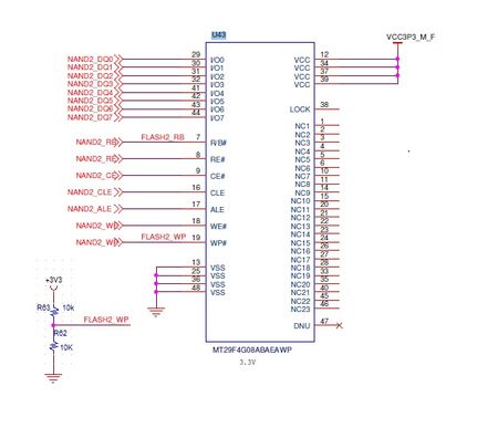

 Frequent Contributor
The short answer: No, connecting WP# to both a 10 kΩ pull-up and a 10 kΩ pull-down simultaneously is incorrect and is very likely the root cause of both the operational failures and the permanent damage you are seeing.
Why the current circuit is harmful
With R63 (10 kΩ to 3.3 V) and R62 (10 kΩ to GND) both permanently connected to WP#, you have a classic voltage divider. When the FLASH2_WP driver is not actively asserting a level, the DC voltage on WP# sits at approximately 1.65 V — squarely in the indeterminate region between the S34ML04G200TFI003's VIL and VIH thresholds. The NAND flash cannot reliably decide whether write protection is asserted or de-asserted. The resulting unpredictable write/erase behavior explains why some devices malfunction during programming; an erase or program cycle that begins with WP# in an indeterminate state can corrupt the internal state machine of the flash and, in the worst case, cause permanent cell damage.
Even when FLASH2_WP actively drives the pin, the pull-down fights the driver when it tries to assert a logic HIGH (VCC through R63 and GND through R62 both load the driver), increasing current and reducing noise margin in both directions.
Correct WP# connection approach
- If write protection is never required at runtime: Tie WP# directly to VCCIO (3.3 V) through a single pull-up resistor (typically 10 kΩ). Remove R62 entirely. The pin will always be deasserted, allowing normal program and erase operations.
- If software-controlled write protection is required: Keep a single pull-up (10 kΩ to 3.3 V) on WP# so the default state is write-enabled, and drive it LOW using an HPS GPIO when protection must be asserted. Never add a simultaneous pull-down — the pull-up alone is sufficient to define the idle state.
- Remove R62 (10 kΩ to GND) from the board. There is no valid use case for a permanent pull-down on an active-low write-protect pin.
Design guideline context
The NAND Flash Interface Design Guidelines for Cyclone V SoC require the external flash device to be an 8-bit ONFI 1.0 compliant device. The NAND flash controller in the HPS also has strict requirements on page size and ECC sector size, and importantly, the NAND interface cannot be exported to the FPGA fabric. NAND Flash Interface Design Guidelines
For the R/B# (Ready/Busy) pin, a related board design note is also worth reviewing: the Cyclone V SoC Pin Connection Guidelines recommend connecting NAND_RB through a 1 kΩ–10 kΩ pull-up resistor to VCCPD_HPS, but for Cypress NAND flash specifically, it is recommended to connect NAND_RB through a 10 kΩ–50 kΩ pull-up resistor to VCCPD_HPS. Why can't Cypress NAND flash be recognized by Cyclone® V SoC FPGAs? Make sure R/B# is also checked — that pin commonly sees similar resistor misconfigurations.
The design guideline also states: ensure that the selected NAND flash device is an 8-bit ONFI 1.0 (or later) compliant device. AN 796: Cyclone V and Arria V SoC Device Design Guidelines Verify that the S34ML04G200TFI003 meets this requirement before continuing board bring-up. You can also check the "Supported Flash Devices for Cyclone V and Arria V SoC" list for confirmed compatible NAND devices. AN 796: Cyclone V and Arria V SoC Device Design Guidelines
Summary action items:
- Remove R62 (the 10 kΩ pull-down to GND on WP#).
- Retain R63 (10 kΩ pull-up to 3.3 V) — or drive WP# actively from an HPS GPIO if runtime protection is needed.
- Verify R/B# pull-up value matches the Cypress/Spansion flash vendor recommendation (10 kΩ–50 kΩ range for Cypress-family devices).
- Any devices that saw WP# in the indeterminate 1.65 V region during erase/program cycles should be treated as potentially damaged and replaced.


