Altera_Forum Honored Contributor
Honored ContributorHonored ContributorHonored ContributorHi,
So this is what I have done so far. I referred to this diagram to create the VHDL code for a D latch (D flip flop later). Link: siddiqleksono.files.wordpress.com/2010/10/d-flipflop_284-nand_1-not29.png (I am sorry I can't post clickable links since I am new here, so kindly paste the link above into your browser.) Unfortunately, simulation result yielded both Q and Q_BAR = HIGH. Can anyone please take a look at my code? Thanks! Refer to the attachment for the VHDL code. Edit: I managed to fix the code, refer to the attachment. Now I need help with creating a D flip flop. For D flip flop, I changed ENABLE to CLK. However, I do not know how to proceed from there. Correct me if I am wrong, for D latch, input = output when ENABLE = 1, whereas for D flip flop, input = output when CLK = rising edge.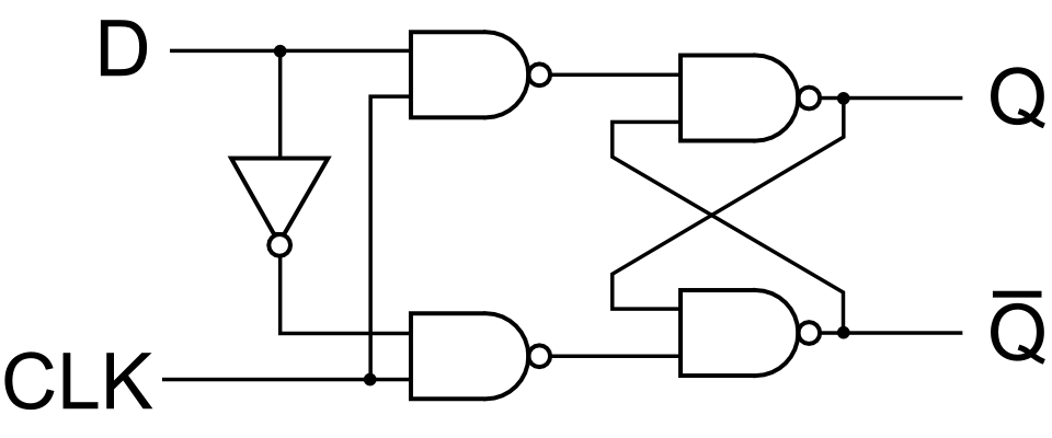