Forum Discussion

 Occasional Contributor
Problem with CXL IP Design Example Type 3 on DK-DEV-AGI027RBES
 2 years ago
Hi again,
The problem was on the PCIe slot on the server side.
We replaced our card and the problem was fixed.
For anyone facing the same problems, we had to check the x16 slot with other devices to identify the lane drop issue in BIOS.
CXL IP designs apparently are note recognized in BIOS as PCIe devices even when the design is working -- the corresponding PCIe slot always shows the message "Link did not train" -- as if nothing is attached on the slot.
Thank you for your help,
Chloe

 Frequent Contributor
Hi Chloe,
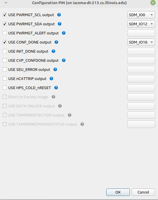
I see. The sw4 should be all off. The error u see about I2C is caused the wrong setting in PMBUS. U can check it in Quartus->Assignment->Device->Device and Pin option, the setting of SCL and SDA in Configuration->Configuration pin option; the setting of VR in Power Management.
The right setting can refer from the setting in example design. Or give me u specific opn of your board, let me check it.
Best regards,
WZ
- xalverti2 years ago
Hi,
Thank you very much for your reply!
So this means that the Table 32 in the document is incorrect?If so could you please then let me know what SW3 should be set to?
Setting SW4 to all off did not make the problem go away.
With respect to the other settings, shouldn't they be already correct? I am compiling the example design for the device.
Our board opn is DK-DEV-AGI027RBES. And we are compiling the type 3 example design for this board.
Best,
Chloe
- xalverti2 years ago
I am attaching some screenshots from our configuration in case that helps.
Thank you,
Chloe