Forum Discussion

 Occasional Contributor
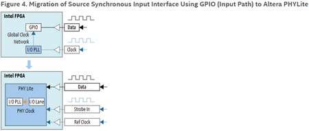
How to migrate source-synchronous GPIO to Intel PHY Lite IP?
 4 years ago
My company was somehow able to contact an engineer at Intel, who solved the problem immediately.
In summary:
- The refclk and strb pins (two FPGA pins) must both be driven by the same external clock.
- There is a bug in all versions of Quartus up to and including 21.4, which prevents the IO delay chains from being configured correctly. Therefore, the design will typically fail timing, even if everything has been configured correctly. As a workaround (until the bug is fixed in Quartus 22.1), the IO delay chains can be configured manually (see details below).
Here is the content of the (excellent) E-mail:
Quartus should automatically change the IO delay chain settings such that each IO is optimized for both setup and hold however there appears to be a problem with the automatic delay chain calculation algorithm in 21.3 which is why you are seeing lots of hold violations while your setup looks good.

I have checked in 21.4 and can confirm that the same issue exists in that version too.
I can however confirm that this issue has been resolved in the latest internal release of 22.1 which is due for release very soon.

As a temporary solution (prior to the release of 22.1) you can manually set the IO delay chain values using the assignment below.

set_instance_assignment -name IO_12_LANE_INPUT_DATA_DELAY_CHAIN 60 -to InData

You can apply this to all InData pins (as in the assignment above) however to get the optimum solution you will need to apply different values on a per-pin basis which is also supported.
I am looking at what specific settings are required to close timing and will update you in due course.

You can see the delay chain values used in the "Delay Chain Summary" section of the Route Stage report.

I tested the assignment above in 21.3 and the interface closed timing.

With regard to the refclk versus the strobe, ideally these should both originate from the same clock source such that they are PPM aligned. This will prevent the internal FIFO within the PHYLITE IP from overflowing/underflowing.
The simplest solution is to connect the same clock on your board to both the strobe and refclk pins of the device.
We applied these changes in our project and it met timing. Correct behavior has been confirmed in simulation.

 Regular Contributor
Hi,
The reference clock should be connected to dedicated clock input pin CLK_xx and Strobe_in should be connected to DQS pins.
For reference you can generate the IP, run fitter and let the tool assign the pins itself. You can then choose similar pins for your final design.
Regards
Occasional Contributor@Ash_R_Intel What is the difference between the reference clock and strobe_in in this case? For a source-synchronous input, aren't they exactly the same thing? (That's why the old GPIO method only needs one clock input).
Also, the reference clock does not have to be connected to a dedicated clock pin. I know this is Intel's recommendation for best timing performance, but it can also be connected to an internally generated (PLL) clock. Therefore, would it not be possible, for example, to run the ref_clk at a higher frequency than strobe_in, then use rdata_valid to identify the valid data?
It would be a huge expense if I need to redesign my PCB just to route the external clock to two pins instead of one. Is there definitely no way to make this work without changing the PCB schematic?

