HBhat2 Contributor
ContributorContributor Regular Contributor
Hi HPB,
My earlier suggestion is to swap tx_parallel_data and rx_parallel_data, the data bus that connect HSSI channel and DP IP together.
From DP IP perspective, by right it won't notice any lane swap effect at all as the lane swap is only happening on board.
I visualize the connection like below, DP RX lane 0 SYNC block should still works as it's interacting with data from lane 0 only all the while. Correct me if I am wrong
Thanks.
Regards,
dlim
ContributorHi,
DP is a 4 lane or 2 lane protocol. To support this we need to enable Bonding in Native PHY IP. There, we are going to mention the master channel. My first concern is if we mention channel 0 is the PCS master, and then the lane swap happens, whether that will create any problem.
Regarding Dynamic Muxing,
Consider Transceiver A -Channel 0- TX is considered as Lane-0 during compile time. and Channel-1 is Lane-1 and so on..
Once FPGA is configured and when I connect DP Sink, then consider it is a non-flip connection, So, Lane-0 of FPGA is connected to Lane-0 of DP sink, Lane-1 of FPGA is connected to Lane-1 of sink and so on..
Now, I connected a 2nd DP sink but with flip connection. With some mechanism I came to know that Type-C is in flip orientation. Now, I must send lane-4 data in channel 0 of Transceiver, Lane-3 data in channel 1, Lane-2 data in channel 2 and Lane-0 data in channel 3
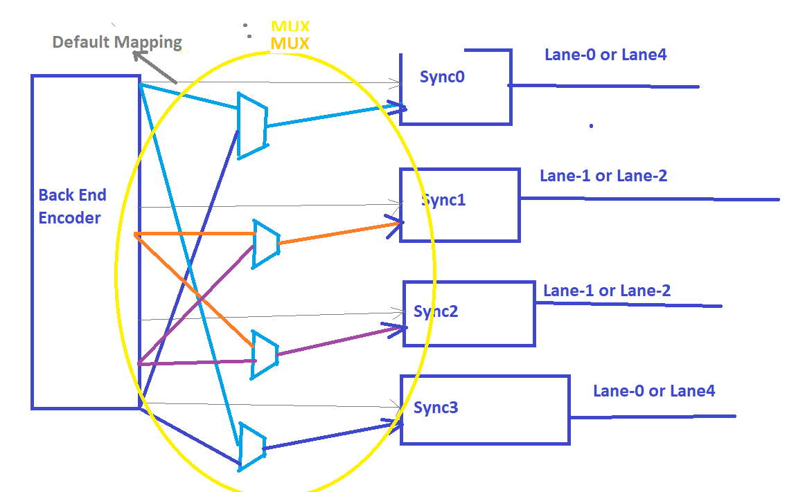
So, to support this I will mux the data coming from the DP Encoder.
The data mux requirement is shown in the attached snapshot.
With Regards,
HPB