Altera_Forum Honored Contributor
12 years agoHonored ContributorJTAG TCK droop using USB Blaster(Ver B) and Cyclone II
I have a NIOS-II processor in a Cyclone II which I am trying to debug using a USB Blaster (Ver B.) cable and The NIOS-II eclipse tools.
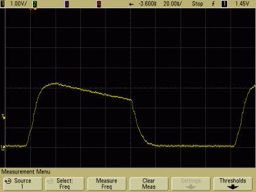
However, the JTAG communications are highly unreliable. VCCIO and VCCA are 3.3V for all IO banks, VCCINT is 1.2V JTAG connections are as follows: TDI and TMS are pulled to 3.3V with 1K resistors TCK is pulled low with a 1K resistor. Pin2 is GND Pin4 is 3.3V Pin6 is tied to 3.3V via a 1K resistor I have tried monitoring the JTAG signals with an oscilloscope. The TDO, TMS and TDI signals all 'seem' to be ok, but the TCK clock looks wrong. I have attached a photo of the TCK signal on the oscilloscope. This shows that it is not a nice square waveform. The frequency is correct (6MHz), but the clock droops from its peak at 3.3V to a level around 2.3V. When it is not clocking, the 'resting state' of the TCK line is this 2.3V. If the USB blaster cable is unplugged, the TCK pin on the PCB drops to 0V, so it is not the PCB which is biasing TCK to 2.3V. Please can you give me some specific hints as to what might be causing this, tests to try, and what I might do to correct it. Thank you. PS: This same USB Blaster is always reliable when programming EPCS devices on other boards.