Altera_Forum Honored Contributor
15 years agoHonored ContributorHow to configure cyclone 3
I have questions to ask.
1.IN the figure, if the VCCIO supply of the bank in which nstatus pin resides is 3.3v,is the nstatus pin pull-up resistors voltages 3.3v in AS MODE?? 2.IN the figure,the TDI pin pull-up resistors voltages is Vcca. DOES Vcca represent voltage (analog) for phase-locked loop (PLL) regulator? Does the TDI pin pull-up resistors voltages have Nothing to do with the VCCIO supply of the bank in which the TDI pin resides in JTAG mode?? the 4 pin voltage is Vcca in JTAG mode ,DOES 4 pin voltage have Nothing to do with everything? the 4 pin voltage is 3.3V in AS mode ,DOES 4 pin voltage have Nothing to do with everything? 3.IF MSEL [3..0]=0100,is the logic '1' Vcca or the VCCIO supply of the bank in which the configuration pins reside? IF MSEL [3..0]=0010,is the logic '1' Vcca or the VCCIO supply of the bank in which the configuration pins reside? thanks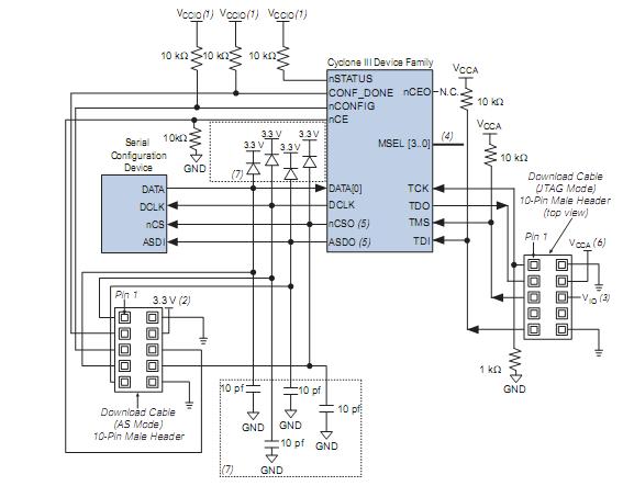