yangz New Contributor
New ContributorNew ContributorNew ContributorHi Yoichi,
Thank you for your response. I noticed that the example design includes only J1 (the DIMM A connector), but not J2 (the DIMM B connector). Is there any documentation available for the pin assignment of J2 as well?
I also noticed that the pin assignments for the AGI 027 (ES) and AGI 027 (ES2) development kits appear to be the same for the J1 far slot, Channel 0, and Channel 1. Is this expected?
 Contributor
Coping from devkit user guide. The slot support only 2-DPC(dual per channel) thus J1 and J2 signals are shared across dual dimms beside CS/ODT/CKE.
The two 288-pin DIMM sockets interface to bank 3C, 3D for Dual DIMM memory.
These sockets accept DDR4 module. These DIMM support dual rank at frequency
1333 MHZ 16 GB per channel, and single rank at 1333 MHZ 8 GB per channel.
— Some board re-work is required for using DIMM sockets in 2-DPC configuration
or different kinds of DDR4 modules. For more details of the resistor
connections required to be present for the type of configuration used, refer to
board schematic table.
Do you want to enable 2-DPC configuration ? or just 1-DPC which can be generated from example design.
New ContributorYes, we want to enable 2-DPC with external DDR4 DIMMs configuration. Is there any reference pin assignment for that?
Contributor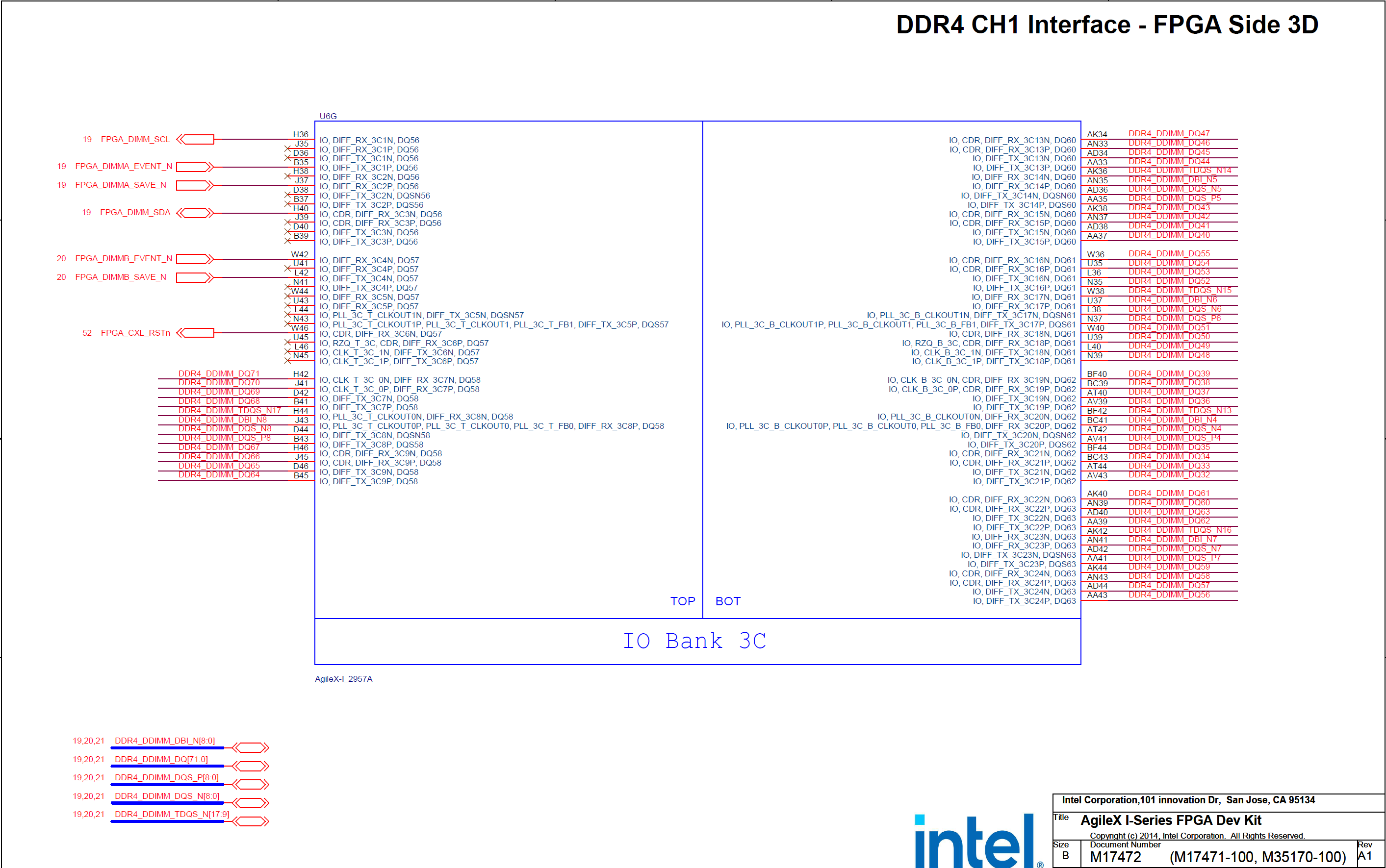
Contributor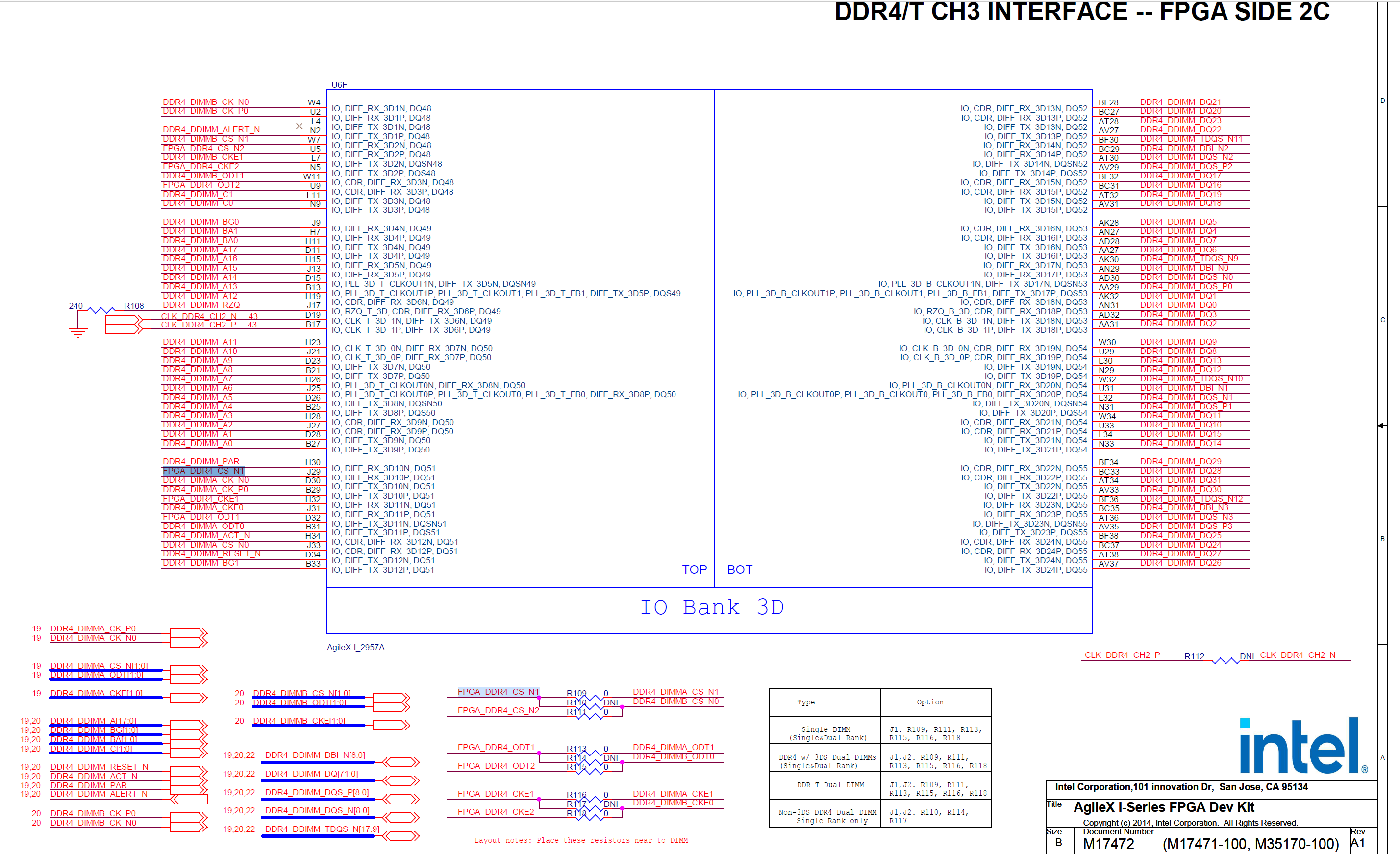
ContributorHere is 3C/3D bank information for you.
New ContributorHi,
Thank you for providing the design file for ddr4_ddimm. I believe we will also need the file for ddr4_ddimm2 to enable the 2-DPC design. Could you please provide that as well?