Altera_Forum Honored Contributor
Honored ContributorHonored ContributorHonored ContributorHere is my design we're going to layout with:
http://i1008.photobucket.com/albums/af207/matthew_db/work/config.jpg?t=1255448620 The 6 net tagged lines going in or out of the 74LV365 are going to GPIO pins over a short ribbon cable. I can use the AT17LV010 during development and as a backup plan. For early production the AT17LV010, the socket and the header would be no place. If this works, they can go at a later version of the board. I went ahead and included both DATA[0] and DCLK since there are extra gates on a hex tri-state buffer.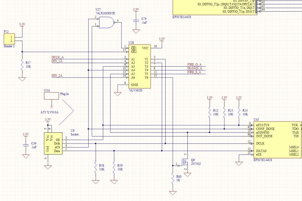