Forum Discussion
 New Contributor
MAX V CPLD Development Kit - Will not work for a simple logic circuit
 Super Contributor
Assuming I have the right board, J6.9 and J6.10 are incorrect for N1 and N2. N1 and N2 are on J6.6 and J6.5 respectively. See page 2-8 here:
New ContributorHell sstrell,
You have the right board.
>> Assuming I have the right board, J6.9 and J6.10 are incorrect for N1 and N2. N1 and N2 are on J6.6 and J6.5 respectively.
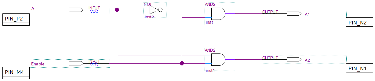
Pins J6.9 and J6.10 are the two AND gate outputs. Also, I accepted the 3.3 LV default. When I test with external switches to the board and outputs to a O-scope, nothing. See attached pictures.
Am I to have additional pins connected. If I am using 3.3 LV, what must be done with the other power level pins?
Thank you.
 sstrell5 years ago
As I stated, N1 and N2 are the MAX V device pin names, but they are actually connected to J6.6 and J6.5, not J6.9 and J6.10. Attach your scope to the correct pins to see the outpu.
 Moe15 years ago
Hello Sstrell,
Will check.
Thank you.
 AminT_Intel4 years ago
Regular Contributor
We do not receive any response from you to the previous question/reply/answer that I have provided. This thread will be transitioned to community support. If you have a new question, feel free to open a new thread to get the support from Intel experts. Otherwise, the community users will continue to help you on this thread. Thank you.
- Moe14 years ago
Hello sstrell,
I been away on work travel. Still on this project, no success.
I am still having problems. A PDF file is provided. The logic circuit is simple. Board not working the way expected.
Thank you.