Forum Discussion
Moe1 New Contributor
5 years agoNew ContributorMAX V CPLD Development Kit - Will not work for a simple logic circuit
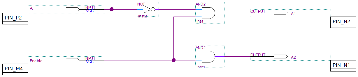
Intel Community, I recently purchased the Max V Development Kit. I figured out how to use the Quartus Prime Lite and successfully installed the Blaster. Created a simple encoder logic circuit, two in...
sstrell Super Contributor
5 years agoSuper ContributorAssuming I have the right board, J6.9 and J6.10 are incorrect for N1 and N2. N1 and N2 are on J6.6 and J6.5 respectively. See page 2-8 here: