Forum Discussion

 New Contributor
I would like to build a connection between my master device and max v, so I program an i2c interface logic to max v which I download from opencores. But I can read from my master device but can't write correctly to the MAX V cpld.

 Regular Contributor
Hi Liam,
Great that the example design did work, I noticed that the example design an494 demonstrate no register address, we do have another example design that have command register:
https://www.intel.com/content/dam/www/programmable/us/en/pdfs/literature/an/an486.pdf
However this example design demonstrate the MAX FPGA devices serve as a bridge between a host that has serial peripheral interface (SPI) to communicate with devices connected through an I2C bus. This may be as close as what you are trying to achieve.
Regards.
 Zhilang_X_Intel7 years ago
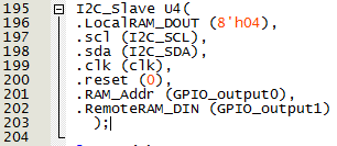
Thanks for your advice. But the an486 example set the MAX FPGA to a master not a slave, and I just set my MAX V to a I2C slave. So could you please help me review my I2C_to_GPIO_modify file?
- EBERLAZARE_I_Intel7 years ago
Hi,
Are you facing the write issue using the code entirely from opencores? I am unsure if the code are supposedly targeted for MAX V device.
I am not really familiar with verilog, but you probably want to get the register address code to work first since the an494 example is already working.
Regards.
- EBERLAZARE_I_Intel7 years ago
Hi,
Are there any update to this issue?
Regards.
- EBERLAZARE_I_Intel7 years ago
Hi Liam,
Since the example code that you shared is not for targeting our MAX V devices, it is difficult to debug why it failed when adding the register address.
I have sent out an example of a design file of MAX V via message, can you check it out?
Regards.