Forum Discussion

 New Contributor
GPIO DDRIO IP output swapped: datainhi/datainlo inverts forwarded clock
 4 years ago
Hello Paul,
We have checked the design. We think it may be because of your coding design. We switched your 10 to 01 and got this result. Is this what you are expecting?
Image 1: Waveform
Image 2: Design
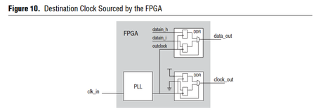
Image 3: Reference from https://www.intel.com/content/dam/www/programmable/us/en/pdfs/literature/ug/ug_altera_gpio.pdf
Thank you.
 Regular Contributor
Hello,
What do you mean by 'I have good reason to believe this is happening with the actual hardware as well, so it isn't just a sim issue'?
Thanks
 New Contributor
The synthesized design behaves as the simulation shows: the signal on datainhi is output on the falling edge of the clock. For my source synchronous interface, this was sneaking in a 180-degree phase shift on the output clock. The timing analyzer assumes pos-unate edges so data transitions occur in the wrong place relative to the active edge of the clock, which breaks my interface. If I swap datainhi and datainlo, my design works as expected.
- AminT_Intel4 years ago
Hello Paul,
We have checked the design. We think it may be because of your coding design. We switched your 10 to 01 and got this result. Is this what you are expecting?
Image 1: Waveform
Image 2: Design
Image 3: Reference from https://www.intel.com/content/dam/www/programmable/us/en/pdfs/literature/ug/ug_altera_gpio.pdf
Thank you.
- pnp4 years ago
Amin,
Thank you for looking into this issue! That is exactly where I ended up: I swapped the din values as you did. I see the waveform you posted from the documentation, but that is for half-rate conversion. We are not doing half-rate conversion in this case.
My issue is that the behavior contradicts the documentation:
from https://www.intel.com/content/dam/www/programmable/us/en/pdfs/literature/ug/ug_altera_gpio.pdf
In this case, datain_width is 1. So
datain_h = din[(2 * 1 - 1):1] = din[1:1] and
datain_l = din[(1 - 1):0] = din[0:0]
which matches what I see in the technology mapped netlist (see my initial post in this issue). The comment at the end of the document states:
which is what I expect to happen, however swapping values in din is required to get the expected behavior.
Thanks,
Paul
- AminT_Intel4 years ago
Hello,
The last screenshot you've given is on Guideline: Swap datain_h and datain_l Ports in Migrated IP which is for migration for your GPIO IP from previous devices to the GPIO IP core. This only applies only for the migration.


