Forum Discussion

 Contributor
AN829 - PCIe BAR[2] to read/write FPGA-EMIF-DDR4 over 1GB area
 5 years ago
I forgot to explain further. In AN829, DDR4 is connected to PCIe DMA port which means DDR4 can only be accessed via DMA control only.
That's why I suggested you to switch to use PCIe IP without enabling the DMA logic insides the IP. Then user can connect PCIe IP directly to memory (like DDR4) and access it.
Thanks.
Regards,
dlim
 Regular Contributor
HI,
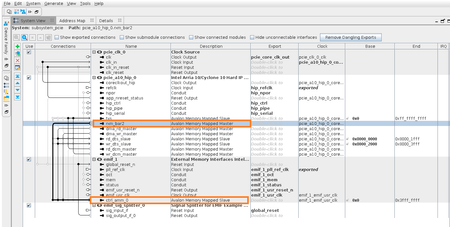
Platform designer only specify offset address, EMIF IP, on chip memory and PCIe IP setting.
Moving data between CPU host memory to FPGA DDR4 memory or on chip memory is controlled by DMA descriptor controller.
- Meaning DMA driver software is the one responsible to configure DMA descriptor to tell it to access which memory address location.
I am not familiar with driver software design but you can try hack DMA driver design DDR4 address offset parameter to see if it helps to change the DMA memory access address to none default 0 address
- Look for altera_dma.h in "AN829_driver" folder
- goto either Arria 10 or Cyclone 10 section (depend on which FPGA product you are using), search for OFFCHIP_MEM_BASE parameter and change it to some other offset value
- Just make sure the new offset value doesn't overwrite with on chip memory address space (ONCHIP_MEM_BASE)
If it still failed, then you will need to study on how to write up DMA driver...
Thanks.
Regards,
dlim
 JET602005 years agoThanks Deshi for answer, We don't wanto engage in DMA operation, What we need is to change some FPGA IP setting to make the PCIE_BAR[2] base address to map to FPGA DDR4 address@0x1000_0000, thus we can use ioread/iowrite to access this part of DDR . Is this possble ? Thanks again


