Altera_Forum Honored Contributor
Honored ContributorHonored ContributorHonored ContributorHello Dave,
interesting. You see, that I didn't scan for all related Altera patents, I found I/O driver the stuff when looking for something different. The current switching topology refers to the standard design for LVDS drivers. It typically has no termination voltage source but a common mode voltage control loop, see the below schematic. You would be able to identify the actual implementation by dynamical measurements, because the common mode control loop would show a reduced bandwidth. On the other hand, the schematic is still a simplification, because it has no programmable termination resistors. Regards, Frank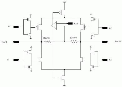