--- Quote Start ---
...The first diagram is just example when clock at register is indeed aligned with pll reference clock.
--- Quote End ---
As I tried to explain: The "cyc5_pll_normal_mode.jpg" diagram is taken directly from the Cyclone 5 manual; it just explains what normal mode should be.
--- Quote Start ---
Moreover, I don't understand your view of "normal", how can a single PLL compensate for any delays to any registers yet having one clock output...or have I misunderstood the concept of delay compensation.
--- Quote End ---
Here is how PLL might be used to do that:
https://www.alteraforum.com/forum/attachment.php?attachmentid=14344 Note: The global clock network should be responsible for making sure that the "CLKOUT" output from the PLL arrives (almost) at the same time at all internal registers.
Note: Cyclone 1 devices seem to be able to exactly achieve the described behavior. TimeQuest of Quartus 9.0 reports a "clock delay path" of close to 0ns (if you compile the design attached as "tpcyc_tco_test.zip" in the original post".
Note: Cyclone 5 devices report a clock path delay of 4.633ns in the slow corner; so the PLL does not seem to compensate much (contrary to what is documented in the manual).
 Honored Contributor
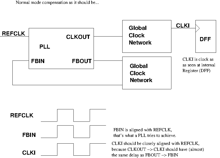