Forum Discussion

 Occasional Contributor
JESD204B rx_islockedtodata signal issue
 2 years ago
Hi,
Yes the root cause is same as you mentioned - no ref clock when FPGA is configured (First time).
Can you please share the reason for configuring LMK04832 via SPI for every power cycle?
Can you program the LMK04832 once and it'll retain the clock configuration? -> If yes Do it.
If not, other solutions:
- Program the FPGA via jic and rbf -> So that even after power cycle FPGA will have its configuration and you just need to give a reset command to FPGA and it'll work. Power up-> FPGA program the clk chip via SPI -> Reset command for FPGA.
- You can implement BMC (Board Management Controller) in your design. BMC will configure the LMK chip first and then bring up the FPGA.
Regards,
HarshX
 Occasional Contributor
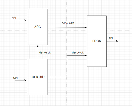
I noticed the reset sequence in the datasheet, which states that before programming the FPGA, stable OSC_CLK_1, management clock, and transceiver reference clock (device clk) are required. However, for my current design, after powering up the board, only OSC_CLK_1 and the management clock are stable. The device clk comes from the clock chip, which needs to be generated through FPGA configuration after I finish configuring the FPGA. I attempted to program the FPGA for the first time and then use the FPGA to configure the clock chip via SPI. At this point, I have stable OSC_CLK_1, management clock, and transceiver reference clock (device clk). Then, I program the FPGA again and configure the ADC via FPGA using SPI to output JESD204B data. rx_islockedtodata can become F, and data reception works properly. Can I achieve JESD204B data reception with only one FPGA programming? Could ADM experts or technical support give some advice? thanks.


