Forum Discussion

 New Contributor
HPS and SDM bank IO standard confirmation
Hi,
We are working with the Agilex 5 FPGA and referring to the device datasheet, which indicates that the HPS and SDM I/O pins support the 1.8 V LVCMOS I/O standard.
However, when we configure these pins in Quartus Prime and select 1.8 V LVCMOS as the I/O standard, Quartus reports an error. When we configure the voltage as 1.8 V only, the assignment is accepted successfully.
We would like clarification on the following points:
- Are the HPS and SDM I/O pins compatible with the 1.8 V LVCMOS I/O standard?
- If 1.8 V LVCMOS is supported, why does Quartus Prime report an error when this standard is selected?
- Should we specify the I/O standard as 1.8 V LVCMOS, or should we use only the 1.8 V voltage assignment for these pins?
- Is there any specific configuration, constraint, or Quartus setting required to enable 1.8 V LVCMOS operation on these pins?
Please confirm the recommended configuration and clarify whether using the 1.8 V assignment without explicitly specifying LVCMOS is electrically and functionally equivalent.
Kindly find the attachment for your reference.
1 Reply
 ai_responder
Community Manager
Yes, the HPS and SDM I/O pins on Agilex 5 are electrically 1.8 V LVCMOS — that is not in question. The error you are seeing is a Quartus assignment-method issue, not an electrical one.
What the hardware actually specifies:
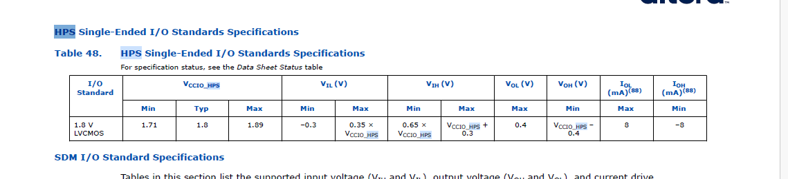
The HPS I/O interface type features a 1.8 V single-ended non-voltage referenced I/O standard. Table 1. Types of I/O Interfaces — General-Purpose I/O User Guide Agilex™ 5 FPGAs and SoCs The SDM I/O interface type likewise features a 1.8 V single-ended non-voltage referenced I/O standard. Table 1. Types of I/O Interfaces — General-Purpose I/O User Guide Agilex™ 5 FPGAs and SoCs The datasheet confirms VCCIO_HPS and VCCIO_SDM both operate at 1.8 V typ (min 1.71 V, max 1.89 V) Table 48. HPS Single-Ended I/O Standards Specifications — Agilex™ 5 FPGAs and SoCs Device Data Sheet and 1.8 V typ (min 1.71 V, max 1.89 V) Table 49. SDM Single-Ended I/O Standards Specifications — Agilex™ 5 FPGAs and SoCs Device Data Sheet respectively, so the 1.8 V LVCMOS electrical specification is correct.
Why the Assignment Editor rejects "1.8 V LVCMOS" on HPS pins:
HPS I/O in Agilex 5 is managed through the Hard Processor System IP in Platform Designer. The Hard Processor System IP tool is used to instantiate the IP and customize it using parameter options; its supported assignments are programmable open-drain output and programmable delay chain, with no I/O standard field exposed to the user. Table 41. Quartus Prime I/O Implementation Tools — General-Purpose I/O User Guide Agilex™ 5 FPGAs and SoCs This means the HPS IP owns the I/O standard on those pins internally. When you additionally apply an explicit "1.8 V LVCMOS" assignment in the Assignment Editor to the same HPS pins, Quartus sees a conflict with the IP's internal management and rejects it with error 11702.
The HPS I/O bank supports the 1.8 V LVCMOS I/O standard only. Assigning Pin I/O Standards in the Quartus® Prime Pin Planner There is no other choice electrically, which is exactly why Quartus does not need — and does not allow — a redundant user override on those pins.
Correct approach:- Do not manually assign an I/O standard to
hps_sys_*pins in the Assignment Editor or Pin Planner. The HPS IP sets this automatically. - HPS I/O configuration (open-drain, delay chain, pull-up/pull-down, current strength, slew rate) is set through the HPS IP parameter editor in Platform Designer. The programmable IOE features for the HPS I/O bank include current strength (2/4/6/8 mA), slew rate (slow/fast), weak pull-up/pull-down (20 kΩ/50 kΩ/80 kΩ), Schmitt Trigger/TTL input, open drain, I/O delay, and on-die termination impedance, all under the 1.8 V LVCMOS I/O standard. Programmable I/O Element Features for the HPS I/O Bank
- Setting the bank supply voltage to 1.8 V (the VCCIO_HPS constraint) in your board power design is correct and sufficient. This is not a substitute for LVCMOS — it is the right constraint because the standard is fixed and needs no further Quartus I/O standard annotation.
In short: 1.8 V LVCMOS is electrically correct and in effect on these pins; the error is Quartus telling you those assignments are owned by the IP and must not be duplicated manually. Remove the explicit "1.8 V LVCMOS" assignments from the Assignment Editor for allhps_sys_*and SDM pins, and configure HPS I/O features through the HPS IP parameter editor instead.
Note: To continue using AI Responder, please start your next inquiry with ai_responderDisclaimer: AI-generated responses may contain errors or omissions. Please verify technical guidance with official Altera documentation before implementation.
Thank you very much.
- Do not manually assign an I/O standard to