Forum Discussion

 Occasional Contributor
EP4CE15U14A7N DDR2 interface
 3 years ago
Hi,
just read the device manual and pin list thoroughly.
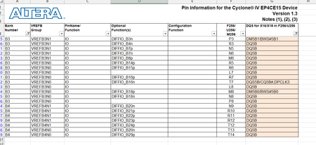
Post #1 is quoting the DQS for x16/x18 column, however as clearly written in the device manual and stated in post #2, DDR2 RAM has to use x8/x9 DQS configuration. There are more DQS pins available for x8/x9, e.g. M7 and T7 in bottom banks B3/B4.
 Occasional Contributor
talk more on it:
Then the only choice to get 16 bit done are to use bank 3 and bank 8 together, but one bank located at top side, the other bank located at bottom side. I am not sure if it's the right way. Generally they should be located nearby bank for one ddr chip.
if I assigned bank3 and bank 4 as ddr and there are still some free 1.8V IO not used, can I assign the free IO for other function?
For example: some bank3 IO are assigned to ddr, some bank3 IO are assigned to spi, general input and output.


