Altera_Forum Honored Contributor
Honored ContributorHonored ContributorHonored ContributorYou should look at your design from a hardware viewpoint. A Verilog or VHDL is synthesizable, if it can be mapped to FPGA harware, particularly logic elements. You'll notice that the FPGA registers have only one clock input, you can't control a register by multiple clocks at the same time.
I understand that you need multiple phase shifted clocks to achieve the intended timing resolution, but it's impossible to output the fast output waveforms or internal signals from a single register. So as a first step you need to sketch a hardware circuit that is able to generate the intended waveforms. Combining multiple register outputs with combinational circuits can be a solution, that's also what the dedicated DDR output registers in Cyclone II and other FPGA families do.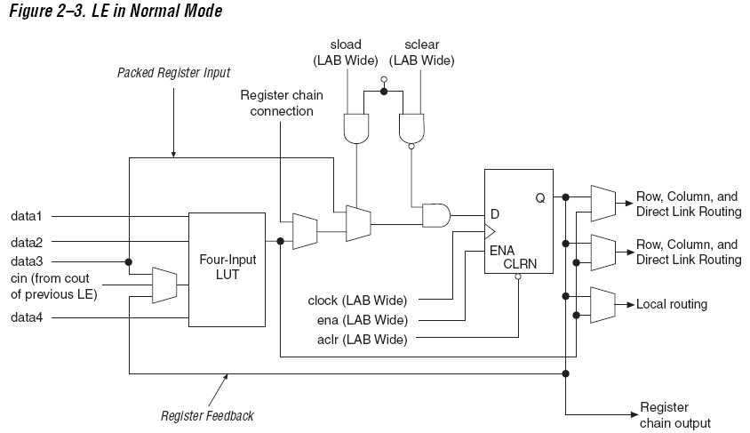