Forum Discussion

 New Contributor
Cyclone V E AS Configuration with MX25L256
 New Contributor
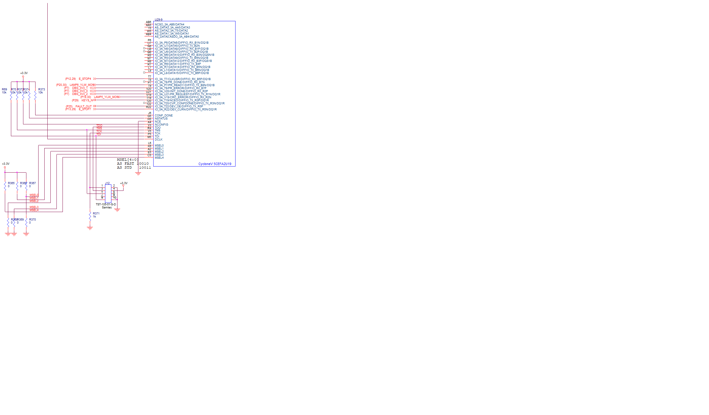
The MSEL pins are connected through zero Ohm resistors. We have tried AS Standard (R370 out and R367 in) and AS Fast(R370 in and R367 out) . I have attached a picture.
New ContributorDo you need a copy of the .JIC file? We have created one with all combinations of the Advanced options and all behave the same.
Disable EPCS/EPCQ ID check
Disable AS mode CONF_DONE error check.
- Bill_A4 years ago
I have attached a picture with the connections to the SPI FLASH
- Bill_A4 years ago
More information.
I have created a custom device to try different settings. Can you get me information about how the programmer sets up the FLASH and the commands that the Cyclone V issues to configure the FPGA.
We tried an ASx1 JIC file and looked at the transactions. The FPGA issued a RDSR (Read Status Register) command and read back 0x40. This indicates that QUAD ENABLE bit is set. This was supposed to be an ASx1 file so I thought that the programmer would have cleared that bit. The FPGA also issues a RDID which returns the expected data. After that, the FPGA reads data and tries to configure. The DCLK changes frequency but the configuration fails.
Does the programmer set values in non-volatile memory in the FPGA to configure the type of SPI FLASH? What should the programming sequence be? I noticed the defaults in the custom device set 4 byte addressing and then turn it off under termination. When we monitored the configuration sequence, we never see 4 byte addressing get enabled.
 Farabi_Altera4 years ago
Regular Contributor
Hi,
I am referring to this link: https://www.intel.com/content/www/us/en/docs/programmable/683271/current/understanding-quad-spi-flash-byte-addressing.html
there is dummy cycle that is required. for 4-byte addressing, 4 dummy cycles is required before the config block controller receiving the valid bitstream.
and I compare with Macronix handbook below, it needs to set DC0 and DC1 accordingly in the configuration register.
and then I compare to AS configuration timing diagram, FGPA need to supply DCLK signal until all bits completely transferred to FPGA.
regards,
Farabi