Open Side Menu
Skip to contentBrand Logo
Forums
BlogKnowledge BaseAltera.com
RegisterSign In
  1. Altera Community
  2. Forums
  3. FPGA Device

Forum Discussion

Altera_Forum's avatar
Altera_Forum
Icon for Honored Contributor rankHonored Contributor
15 years ago

Altera USB-Blaster JTAG Pinout

Hey folks,

Here is the pinout diagram for the Altera USB-Blaster JTAG cable as well as the USB box IDC socket.

http://www.digital-circuitry.com/IMAGES/webpage/MyLAB/Thumb/Altera_USB-Blaster_JTAG_pinout.jpg

hi-res copy (1200 x 645 pixels):

http://www.digital-circuitry.com/images/webpage/mylab/altera_usb-blaster_jtag_pinout.jpg (http://www.digital-circuitry.com/images/webpage/mylab/altera_usb-blaster_jtag_pinout.jpg)

Regards,

-Gerry

http://www.digital-circuitry.com/index.htm (http://www.digital-circuitry.com/index.htm)
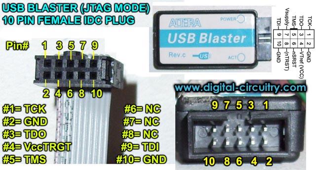
1 Reply

  • Altera_Forum's avatar
    Altera_Forum
    Icon for Honored Contributor rankHonored Contributor
    15 years ago

    And in the user manual (http://www.altera.com/literature/ug/ug_usb_blstr.pdf) on page 2-4 you also have the pinout for the (less used) AS and PS modes.

Recent Discussions

  • FabriceNs's avatar
    FPGA issue on electronic board
    1 day ago
    FabriceNs
  • vasakpal's avatar
    MAX10 RSU upgrade succeeds, but device boots Factory image instead of Application
    1 day ago
    vasakpal
  • FabianL's avatar
    Arria 10: Remote Update Factory Fallback won't work & Watchdog does not trigger
    1 day ago
    FabianL
  • patrick03's avatar
    Max10 FPGA Programming with .pof file
    1 day ago
    patrick03
  • JLIU45's avatar
    About ALTIOBUF simulation
    1 day ago
    JLIU45
Contact Us
Altera YoutubeAltera YoutubeAltera Twitter
  • Company Overview
  • Newsroom
  • Our Leaders
  • Careers
Subscribe to Altera Newsletter

© Altera Corporation | Terms of Use | Privacy Policy | Cookies | Trademarks | PSIRT

Altera Logo